Use Application-Specific Battery PMICs to Get Designs Finished Quickly
投稿人:DigiKey 北美编辑
2017-10-26
Designers of battery powered systems have many power management ICs (PMICs) to pick from to get the right balance of efficiency, performance, footprint, and cost. However, they must also get their designs out the door quickly; so instead of spending too much time in the selection process, they can use application-specific, more highly optimized solutions for a given class of design objectives and priorities.
Broad line PMIC vendors saw that designers struggled to shorten the time taken to select from thousands of general purpose PMICs from dozens of sources, and then add circuitry to optimize those PMICs for their specific applications. To help, they identified unique features and attributes they can add to the PMICs to make application-specific, more highly optimized solutions for a given class of design objectives and priorities.
By choosing a PMIC that is tailored to the needs of a given situation, designers find their task simplified and their BOM and costs reduced, while also achieving better performance. As a further benefit, the designer does not need to try to adapt the PMIC to the situation, thus saving time and minimizing frustration.
This article will review the basic roles of a PMIC. It will then look at five disparate PMIC challenges and describe solutions that greatly reduce design time, effort, and aggravation.
The role of a PMIC
There is no single, universally accepted definition of a PMIC or its roles because the power needs of systems vary so widely. In general, a PMIC is responsible for one or more of these roles:
- Function as voltage buck, boost, or buck/boost converter
- Ensure that regulated current is delivered from the source to the load at the right voltage
- Manage the discharging of primary (non-rechargeable) and secondary (rechargeable) cells, as well as the charging of secondary cells
- Manage the DC rail output when it is being supplied by a battery, and doing so while the battery is being charged, if applicable
- Ensure that ramp up/down timing and sequencing among multiple rails is done correctly
- Prevent power-subsystem or battery condition and faults (internal short, fully discharged, or absence) from causing system-wide damage, and vice versa
But these are just starting points for PMIC functionality. As electronic devices and systems have spread into countless applications – many of which barely existed a few years ago – PMIC suppliers have addressed the unique needs of each niche by adding targeted functions and features, as well as emphasizing certain performance parameters to best match these niche needs.
The USB design challenge
The USB specification has gone through several major upgrades that have boosted its speed, and made it a very widely used DC power source with current ratings that range from 0.5 amperes (A) to 5 A.
PMIC design challenge #1: Use a USB interconnection to charge a battery and also provide circuit power.
USB has become the near universal charging source of choice for many devices. The design challenge has been to provide the DC/DC power rail regulation from the USB port acting as the power source, and also manage this power to charge an internal battery in many cases. Doing so requires more than just voltage conversion and regulation, it also requires management of the cell charge/discharge profile. The latter can be very complicated, with specifics that depend upon the chemistry.
A design must also be in compliance with the specifications and protocol of the USB standard, including port detection and setup, charging of a dead battery, tolerating spikes due to insertion/removal of the USB connector, and operating with all USB compliant sources.
PMIC solution: An IC such as the Analog Devices ADP5065 fast-charge battery manager with power path and USB compatibility can meet these needs (Figure 1). It operates from an input voltage between 4 volts and 5.5 volts, yet can also tolerate voltages of up to 20 volts, to minimize issues associated with USB bus “spiking.”
Figure 1: The ADP5065 from Analog Devices solves multiple issues related to USB-based battery charging, seamless operation from battery or USB power, and absent or discharged battery. (Image source: Analog Devices)
The DC/DC switching device operates at 3 megahertz (MHz), providing up to 1.25 A of charge current from a dedicated charger. The internal FET between the charger output and the battery provides isolation, allowing it to still deliver power to the system even if the battery is dead or absent.
To do so, the IC implements the USB protocol sequence for both battery presence detection and dead battery detection, critical to meeting USB operational standard (Figure 2 and Figure 3). This allows for immediate system operation from the USB supply, without the need for a viable battery in place.

Figure 2: The ADP5065 charger actively sinks and sources current into a specific IC node, and voltage vs. time is detected. The sink phase is used to detect a charged battery. (Image source: Analog Devices)

Figure 3: The source phase is used to detect a discharged battery by injecting a current for a limited time, and checking the response. If specific criteria are met, the IC charger assumes that a battery is present, and begins a new charge cycle. (Image source: Analog Devices)
Using the I2C port of the ADP5605, a system processor can program all critical charge/discharged parameters including trickle charge current level, trickle charge voltage threshold, weak charge (constant current) current level, fast charge (constant current) current level, and fast charge (constant voltage) voltage level, among others.
PMIC design challenge #2: Detect, manage, and protect a USB port in almost any scenario.
PMIC solution: Another PMIC with USB attributes is the PI3USB9281C from Diodes Incorporated. This device provides external detection for any USB device. It can detect any of the wide range of available chargers, including Mobile High-Definition Link (MHL) accessories, OTG (On the Go) accessories, and car chargers, per CEA-936-A (USB Carkit Specification), a CEA standard that allows the use of a mini USB connector for UART and analog audio signals. It also integrates a power switch with over-voltage and over-current protections (Figure 4). The VBUSIN input pin can tolerate voltages up to 28 volts, which is important for USB 3.0 Power Delivery enabled ports.
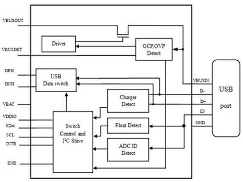
Figure 4: Using the PI3USB9281C, designers can easily implement a charger that detects and then operates from almost any USB source. (Image source: Diodes Incorporated)
The flowchart shows the complexity of the USB handshaking and interface when a device is connected (Figure 5). By adding this to its other PMIC functions, this IC manages charging of integrated Li-ion batteries via USB connectors. If this flowchart’s sequence is not implemented by the IC, the designer would have to code it into the system microcontroller. This is a time-consuming, error-prone process that would still need USB certification.
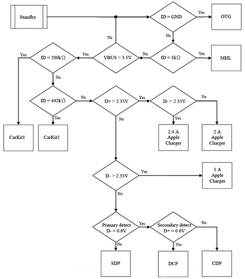
Figure 5: Detecting what type of USB port and source is connected and assessing its validity is not simple, as this flow chart (state diagram) for the PI3USB9281C, demonstrates. (Image source: Diodes Incorporated)
Buck, boost operation: another PMIC role
Although there are many applications which only need voltage conversion and regulation solely in buck mode or boost mode (voltage step-down or step-up, respectively) there are also many that need both transformations. In these cases, the PMIC must not only provide the buck and boost functions, but often also manage a seamless transition between the two modes. This would be the case, for example, where a single Li-ion cell must be managed to deliver a 2.0 volt rail as that cell drains from fully charged at 2.6 volts, down to a fairly depleted 1.6 volt output.
PMIC design challenge #3: Provide charge/discharge management for almost any battery chemistry
PMIC solution: To address various chemistries in a single design, ICs such as the Texas Instruments bq25703A can be used. This I2C multi-chemistry battery buck-boost charge controller also includes a system power monitor and a processor hot monitor. It accepts a 3.5 volt to 24 volt input operating voltage, and supports charging of battery packs of almost any chemistry (Li+, LiFePO4, NiCad, NiMH, lead acid) with one to four cells (Figure 6). Target applications include consumer products such as drones, Bluetooth speakers, IP cameras, laptops, and tablet PCs, as well as industrial and medical equipment.
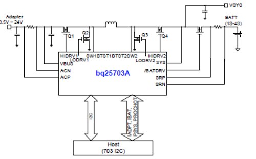
Figure 6: The bq25703A provides charger management for all standard battery chemistries; it functions from a wide range of power sources between 3.5 volts and 24 volts, while supporting battery packs of one to four cells. (Image source: Texas Instruments)
Its primary function is to charge the battery from a wide range of input sources including USB adapters, high-voltage USB PD sources and traditional adapters. It can also keep the system (the load) operating even when the battery is completely discharged or removed. The small size of this IC – a 32-pin 4 × 4 WQFN – means that it can be housed within the battery pack for enhanced system integrity and reliability.
It is also sophisticated enough to provide instant-on, even with no battery or a deeply discharged battery (a common occurrence), and also let the battery supplement the system when the charging adapter is fully loaded. The power-up timing of key signals on the bq25703A in a two-cell, no-battery configuration, with a 20 volt source, is shown in Figure 7. It shows a crisp transition of about 10 milliseconds (ms) for the output voltage bus, without overshoot or ringing.
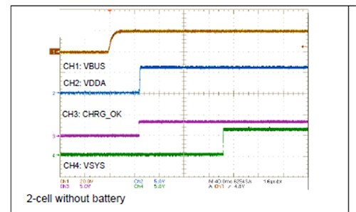
Figure 7: The power-up timing of key signals on the bq25703A with a two-cell, no-battery configuration, with a 20 volt source. (Image source: Texas Instruments)
With a 5 volt source, the output voltage takes about 35 ms to reach final voltage (Figure 8).
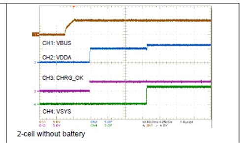
Figure 8: The power-up timing of key signals on the bq25703A with a two-cell, no-battery configuration, with a 5 volt source. (Image source: Texas Instruments)
PMIC design challenge #4: Manage charge/discharge/sharing of higher voltage batteries with widely differing rails in dual battery supplies, such as automotive 12/48 volt systems.
PMIC solution: Another power related design issue involves the use of dual voltage busses in automobiles, a change that applies to standard internal combustion vehicles as well as all-electric and hybrid vehicles (EV/HEV). The present 12 volt battery and bus cannot supply enough current and power without incurring severe voltage losses due to current-resistance (IR) drop and power losses due to I2R dissipation, respectively. While these losses can be reduced using heavy-duty cabling and connectors, this option adds weight, space, and cost.
Alternatively, the auto industry is settling on a new dual bus standard, which supports both 48 and 12 volt, busses simultaneously. However, managing these dual busses and optimizing their ability to deliver power efficiently, while charging the batteries properly, is a difficult design task.
To resolve the issues, one option is to use the LTC3871 from Linear Technology Corp. (now part of Analog Devices). This is a high-performance, bidirectional, switching regulator controller that operates in either buck or boost mode on demand, making it a good fit for 48/12 volt automotive dual battery systems (Figure 9).
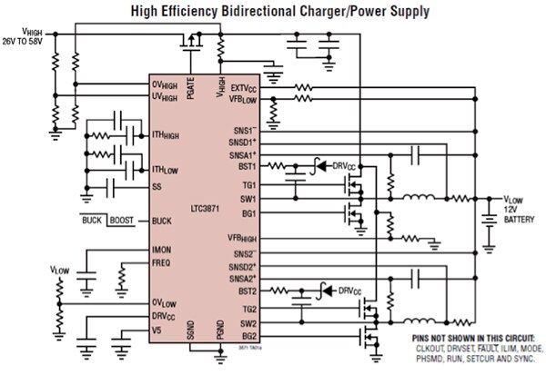
Figure 9: Managing the charging, discharging, and sharing of an automotive 48 and 12 volt battery system requires a bidirectional, buck/boost PMIC, such as the LTC3871. Image source: Linear Technology Corp.)
An accurate current programming loop regulates the maximum current that can be delivered in either direction. The LTC3871 also allows both batteries to supply energy to the load simultaneously. Its architecture allows dynamic regulation of input voltage, output voltage, or current, with voltages up to 100 volts for the higher voltage supply and up to 30 volts for the lower voltage supply. This is well within the requirements of 48 and 12 volt dual bus systems. The LTC3871 also manages a nearly seamless, bump-free transition from buck to boost mode in about 50 microseconds (µs) (Figure 10).
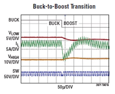
Figure 10: As the LTC3871 shifts from buck to boost mode, the transition is nearly seamless, taking only about 50 µs and showing almost no ringing. (Image source: Linear Technology)
Since this PMIC is specifically targeted at automotive applications, it must meet that industry’s very stringent specifications for the transistor junction temperature operating range (–40°C to 150°C), as well as immunity to transients, load dumps, and other effects on the power rail. It achieves the temperature mandate in part through its use of a 48-lead, 7 mm2, LQFP plastic package with an exposed underside thermal pad for enhanced heatsinking to the pc board.
Micropower also brings PMIC challenges
PMIC design challenge #5: Manage charge/discharge of severely power-constrained wearable device, and keep quiescent current to a minimum.
At the other end of the power and voltage spectrum from automobile batteries are PMICs for ultralow-power applications such as wearables. Here, the critical factors are high efficiency, careful management of various operating modes, optimized battery charging/discharging, and extremely low quiescent current and sleep-mode dissipation.
ICs such as STMicroelectronics’ STBC02JR USB-based Li-ion battery charger, LDO, and load switches address this specialty niche (Figure 11). This highly integrated power management IC also includes a smart reset/watchdog block, and a protection circuit module (PCM) to prevent the battery from being damaged under fault conditions.
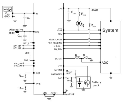
Figure 11: Designed for extreme low-power applications, such as wearables, the STBC02JR emphasizes low standby and quiescent power dissipation. (Image source: STMicroelectronics)
The STBC02 draws less than 10 nanoamps (nA) from the always-connected battery in “shipping-mode” conditions, to maximize the battery shelf life; quiescent current is 600 µA when the unit is in use, yet not connected to a charger. The IC controls battery charge/discharge, and its LDO wakes up from shutdown mode to battery mode (normal use) in about 200 µsec (Figure 12).
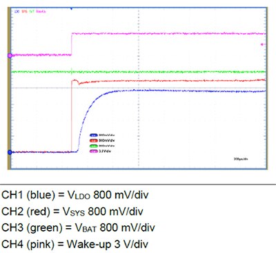
Figure 12: On wakeup, the STBC02JR system output (red) and LDO output (blue) transition nearly simultaneously to full output in about 200 µs, with a brief 20 µs overshoot of about 200 mV on the system output rail, and none on the LDO output. (Image source: STMicroelectronics)
Along with power consumption, size is also critical, so the device comes as a 30-bump flip chip measuring just 2.59 × 2.25 mm. Also, due to the somewhat electrically exposed environment in which it will be used, with the possibility of static electricity from user clothing and other sources, the STBC02 features ±4 kilovolt human body model (HBM) ESD protection on its most critical pins.
Some selection tips
Even with specialized, application-specific ICs, the range and depth of available PMICs can be intimidating, but need not be so. First, discard those where the basic specifications don’t match the top-tier requirements of the application (voltage in, voltage out, current). Then, narrow the search further by looking at the application-specific functions they offer which target unique application issues, such as:
- Battery charging/discharging, protection
- USB connectivity
- Operation with/without battery
- Physical size
Also, note that despite their small size, the multifaceted functionality of these ICs requires studious analysis of data sheets, paying attention to charts, tables, application information, efficiency data, models, and much more.
Look for how to address derating and thermal issues, start-up and transition-mode timing, use of various registers, transients and noise issues, efficiency in various modes, pc board layout guidelines, and suggestions for passive components, as needed.
Conclusion
Designers face many choices when it comes to PMICs, but by opting for application-specific solutions they can reduce time to market, lower cost, and incur fewer headaches and system design “surprises.” However, pay close attention to the often-extensive data sheets in order to realize the potential benefits of these problem solving, application-targeted PMICs.

免责声明:各个作者和/或论坛参与者在本网站发表的观点、看法和意见不代表 DigiKey 的观点、看法和意见,也不代表 DigiKey 官方政策。


