USB 3.1/USB Type-C
2016-02-18
Universal Serial Bus (USB) is a standard developed in the mid-1990s to standardize the connection between computers and peripherals, both to communicate and to supply electrical power. It replaced a variety of earlier interfaces such as serial/parallel ports, PS/2, and separate power chargers for portable devices.
There are three connector sizes – standard, mini, and micro, type “A’, “B”, and “AB” connectors and corresponding receptacles, and five data transfer modes summarized in Table 1:
| USB Type | Throughput | Direction | Total Capacitance | Pin Count |
| 1.X | 1.5 Mbit/s (Low speed) 12 Mbit/s (Full speed) |
Half Duplex; Not reversible | < 30pF | 4 |
| 2.0 | 480 Mbit/s (High Speed) | Half Duplex; Not reversible | < 10pF | 4-5 |
| 3.0 | 5 Gbit/s (SuperSpeed) | Full Duplex; Not reversible | < 1pF | 9 |
| 3.1/Gen2 | 10 Gbit/s (SuperSpeed+) | Full Duplex; Not reversible | < 0.1~0.5pF | 9 |
| Type-C | 10 Gbit/s (SuperSpeed+) | Full Duplex; Reversible | < 0.1pF | 24 |
Table 1: USB data transfer modes.
USB 3.1/Gen 2 is essentially USB 3.0 with double the speed, to 10 Gbit/s. It is full duplex and not reversible, so the connector and receptacle has to be aligned in the correct orientation to be inserted. It has a total capacitance of 0.1 ~ 0.5 pF.
USB Type-C is 10 Gbit/s and reversible (similar to Apple’s Lightning) with symmetrical 24 pins so the connector will attach to the receptacle on the first try. The additional pins permit support of data protocols such as DisplayPort 1.3, PCI Express, and Base-t Ethernet using Type C cables. Figure 1 shows the pinout diagram of USB Type-C cable.
USB Type-C’s connector and receptacle are smaller sized (similar to Lightning and Micro-USB) and more durable, withstanding 10,000 insertion/removal cycles. The cable supports a USB power Delivery mode of up to 100 W, which charges smartphones and tablets much faster. Devices that currently accommodate USB Type-C cable are Apple’s 2015 MacBook, Google’s Chromebook Pixel, Nokia’s N1 tablet, smartphones such as OnePlus 2 and Le Superphone, and mobile storage devices by LaCie and SanDisk.
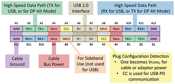
Figure 1: USB Type-C pinout diagram.
Comchip has many low capacitance ESD surge suppressors for USB port protection. Recommended parts for USB 3.0 are in listed in Table 2 and suggested PCB layouts are shown in Figures 2 and 3. Suggested parts and layouts for USB 3.1 are shown in Figures 4 and 5. Recommended parts for Type-C are listed in Table 3 and the suggested flow-through PCB layout is in Figure 6.
USB 2.0 D+, D- (USB 2.0 and 3.0 data lines are combined into one)
| Part Number | VRWM | IR (Max) | VC | Cj | ESD (Contact) | Package |
| CPDQR5V0USP-HF | 5 V | 1 μA | 13 V | 0.6 pF | ±8 KV | 0402 1-Line/Uni |
| CPDQ5V0USP-HF | 5 V | 1 μA | 13 V | 0.6 pF | ±8 KV | 0402 1-Line/Uni |
| CPDQC5V0USP-HF | 5 V | 1 μA | 13 V | 0.6 pF | ±8 KV | 0402C 1-Line/Uni |
| CPDU5V0USP-HF | 5 V | 1 μA | 9.8 V | 0.5 pF | ±10 KV | 0603 1-Line/Uni |
| CPDUC5V0USP-HF | 5 V | 1 μA | 9.8 V | 0.5 pF | ±10 KV | 0603C 1-Line/Uni |
| CPDT-5V0UP-HF | 5 V | 1 μA | 12 V | 0.6 pF | ±10 KV | SOT-23 2-Line/Uni |
USB 3.0 Tx, Rx
| Part Number | VRWM | IR (Max) | VC | Cj | ESD (Contact) | Package |
| CPDQC5V0CSP-HF | 5 V | 100 A | 15 V | 0.3 pF | ±8 KV | 0402C 1-Line/Bi |
| CPDQC5V0USP-IPHF | 5 V | 100 nA | 12 V | 0.3 pF | ±10 KV | 0402C 1-Line/Uni |
| CPDA10R5V0P-HF | 5 V | 50 nA | 9 V | 0.25 pF | ±18 KV | DFN10P 4-Line/Uni |
VBUS 5V
| Part Number | VRWM | IR (Max) | VC | Cj | ESD (Contact) | Package |
| CPDQC5V0R-HF | 5 V | 90 nA | 8 V | 24 pF | ±30 KV | 0402C 1-Line/Bi |
| CPDUR5V0R-HF | 5 V | 90 nA | 8 V | 24 pF | ±30 KV | 0603 1-Line/Bi |
| CPDUC5V0R-HF | 5 V | 90 nA | 8 V | 24 pF | ±30 KV | 0603C 1-Line/Bi |
| CPDQR5V0HE-HF | 5 V | 1 μA | 11 V | 15 pF | ±30 KV | 0402 1-Line/Bi |
| CPDQC5V0HE-HF | 5 V | 1 μA | 11 V | 15 pF | ±30 KV | 0402C 1-Line/Bi |
| CPDUR5V0HE-HF | 5 V | 1 μA | 11 V | 15 pF | ±30 KV | 0603 1-Line/Bi |
Table 2: Recommended parts for USB 3.0.
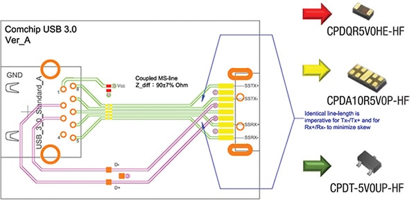
Figure 2: USB 3.0 suggested PCB layout diagram using three components.
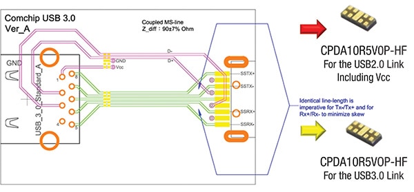
Figure 3: USB 3.0 suggested PCB layout diagram using two components.
USB 3.1 Type A has similar ESD requirements to USB 3.0 Type A, so the suggested PCB layouts are the same, except lower capacitance ESD components are recommended. Suggested PCB layouts for USB 3.1 are shown in Figure 4 and 5.
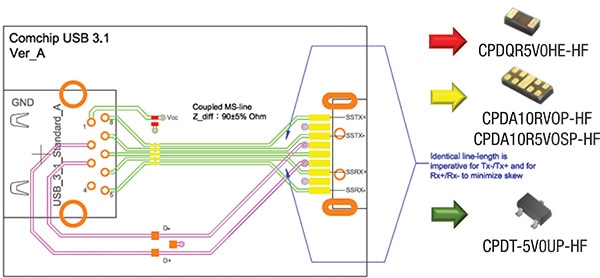
Figure 4: USB 3.1 suggested PCB layout diagram using three components.
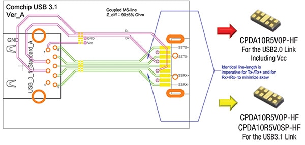
Figure 5: USB 3.1 suggested PCB layout diagram using two components.
USB Type-C has 10 Gbit/s throughput, so ESD protection is essential considering the potential impact of additional capacitance and inductance on the high-speed differential pairs. Due to the reversible connector design, USB Type-C has increased ESD protection requirement.
In such an instance, a flow-through design of Comchip’s DFN10P package simplifies PCB layout by placing the package on top of the high-speed differential pair, avoiding complicated vias or loops and saving PCB space. Recommended parts for USB Type-C are in listed in Table 3 and the suggested PCB layout is shown in Figure 6.
| Part Number | VRWM | IR (Max) | VC | Cj | ESD (Contact) | Package |
| CPDA10R5V0P-HF | 5 V | 50 nA | 11 V | 0.25 pF | ±14 KV | DFN10P 4-Line/Bi |
| CPDA10R5V0SP-HF | 5 V | 50 nA | 12 V | 0.15 pF | ±14 KV | DFN10P 4-Line/Bi |
Table 3: Recommended parts for USB Type-C.
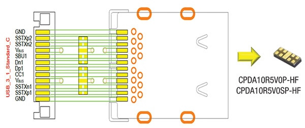
Figure 6: USB Type-C suggested PCB layout diagram with flow-through design.
免责声明:各个作者和/或论坛参与者在本网站发表的观点、看法和意见不代表 DigiKey 的观点、看法和意见,也不代表 DigiKey 官方政策。


