Understanding Switching Regulator Control Loop Response
投稿人:电子产品
2015-09-15
A switching DC-DC voltage regulator (“switching regulator”) relies on a closed feedback control loop to ensure the desired voltage and current output is maintained under varying load conditions. The performance of this control loop influences key performance parameters of the power supply including line- and load-regulation, stability, and dynamic response.
Engineers can quantify the performance of the control loop by measuring the frequency response of the voltage regulator across a wide range of frequencies. The frequency response can then be “tuned” by incorporating compensator networks into the circuit. If the job is done well, the end result is a switching regulator that’s stable over a wide frequency range yet is not overcompensated so that its dynamic response is poor.
This article describes the fundamentals of a switching regulator’s control loop and then looks at some examples of well-designed modular switching controllers and regulators that can be used as the basis of a high-performance power supply.
The voltage regulator control loop
Feedback control loops are simple concepts. The purpose of a control loop is to constrain a system variable (for example, an output) such that it is maintained at a desired value. The system variable is constantly monitored and compared with a reference value, which is equal to the desired output. The error signal (the difference between the desired value and the actual output) is then used to adjust the system variable to bring it back into line.
In a switching regulator the system variable is voltage (and/or current) which is compared with a reference value set by the circuit designer. The output from the error amplifier (the error signal) is then fed into a comparator that adjusts the duty cycle of the switching transistor. The duty cycle is proportional to the output voltage. Figure 1 shows a simplified schematic of the feedback loop for a step-up (“boost”) switching regulator.
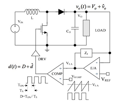
Figure 1: Simplified schematic of control loop for a boost regulator. (Courtesy of Fairchild Semiconductor)
In a perfect control loop, the output voltage would remain locked to the reference voltage no matter what happens to the load or input voltage. In a practical circuit, changes to load and input voltage perturb the output to some degree. The engineer looks to design his or her circuit so that the control loop responds to changes as quickly as possible and regulates the output voltage precisely, yet remains stable.
Control loops can be characterized by their frequency response. The frequency response indicates how a switching regulator will react (determined by the voltage regulator’s “transfer function”) under defined operating conditions across a range of frequencies. The frequency response is a dynamic model of the voltage regulator showing how variations in the input voltage, the load, and duty cycle affect the output voltage according to frequency. The frequency response influences the voltage regulator’s reaction time, precision, and stability.
Gain and phase difference
The frequency response of a circuit can be determined from either mathematical modeling or testing of an actual design (or a combination of both). Neither method is trivial, but voltage regulator manufacturers provide helpful application notes and online software to assist with both techniques. (For example, the Texas Instruments (TI) Application Report1 is a useful guide to a practical measurement technique.)
The Nyquist stability theorem can be used to characterize the frequency response of a control loop, but it is a complex analysis and requires a high level of expertise to extract design insight. Fortunately, switching voltage regulators inevitably include a low-pass filter at the output stage that simplifies the frequency response such that Bode plots can be used to describe the transfer function in place of Nyquist data. Bode plots are easier to analyze than the polar plots generated by Nyquist analysis.
A Bode plot is a graph of magnitude and phase of the transfer function as a function of frequency, where magnitude is plotted in decibels and phase in degrees, respectively, while the frequency is shown on a logarithmic scale. Figure 2 shows gain and phase Bode plots for the boost regulator shown in Figure 1.
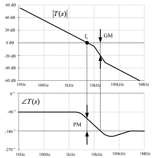
Figure 2: Gain and phase Bode plots for boost voltage regulator. (Courtesy of Fairchild Semiconductor)
These plots reveal some key information about the control loop’s performance. The first point of interest is the crossover frequency (fc). This is the frequency at which the control loop gain is unity (0 dB) and is also referred to as the loop bandwidth (approximately 7 kHz for this example). The second point of interest is the place at which the phase lag reaches 180o (approximately 25 kHz for this example). The phase margin (PM) equals 180o minus the phase lag at fc (approximately 60o for this example). The gain margin (GM) is the gain at a phase lag of 180o (20 dB in this case).
Assuming the gain plot crosses unity (0 dB) only once (which for voltage regulators with a low-pass filter at the output stage is virtually always the case), the system will be stable if the phase lag at fc is less than 180 degrees. At other frequencies, the phase lag can exceed 180o and the control loop will still remain stable. For most control loops experienced engineers aim to achieve a phase margin greater than 45o (and less than 315°). Typically, a phase margin of 45o provides good transient response with good damping. For boost or buck-switching regulators the gain margin should be above 10 dB.
Many systems can be stable for gains greater than 0 dB even though the control loop phase lag is more than 180o for frequencies less than fc. However, such systems can then become unstable when the loop gain decreases. These systems are only “conditionally” stable and do not exhibit good design practice.
(Note that at low loads most switching regulators will enter a discontinuous current conduction mode. In this mode the circuit’s frequency response will change. Also note that voltage mode converters without input voltage feed forward will exhibit a change in frequency response with changes in input voltage. [See the TechZone articles “The Difference Between Switching Regulator Continuous and Discontinuous Modes and Why It's Important” and “Voltage- and Current-Mode Control for PWM Signal Generation in DC-to-DC Switching Regulators”.])
There is a better than even chance that an initial circuit layout will prove unsuitable and to alter the frequency response of a circuit an engineer will need to introduce compensation networks. The task of these networks is to shape the control loop gain such that fc moves to a suitable position and the phase- and gain-margins lead to good dynamic response, line- and load-regulation, and stability. There are several types of compensation networks and these will be discussed in another TechZone article.
A well-designed switching voltage regulator is both electrically and acoustically quiet. This is not the case for undercompensated systems that can exhibit audible noise from the magnetic components or ceramic capacitors, jitter in switching waveforms, oscillation of output voltage, and numerous other undesired characteristics.
On the other hand, an overcompensated system can be very stable and quiet, but at the cost of a slow dynamic response. The fc of such a system will occur at a low frequency, typically below 10 kHz. Slow-dynamic response designs require excessive output capacitance to meet transient regulation requirements, increasing the overall cost and size of the power supply. The trick is, of course, to strike a balance. An optimally compensated design is stable and quiet, but also has a fast response with minimal output capacitance.
Using a power module
While there are some advantages to designing a switching regulator from scratch (see the TechZone article “DC/DC Voltage Regulators: How to Choose Between Discrete and Modular Design”), many engineers base their power supply designs on power modules from semiconductor vendors like Fairchild Semiconductor, Linear Technology, TI, and Maxim Integrated.
Power modules integrate many of the circuit’s elements of a voltage regulator design into a single chip. For example, controllers integrate the error measurement and Pulse-Width-Modulator (PWM) systems (which set the duty cycle) while regulators add switching drivers and the switching elements themselves to the controller circuitry. Often the engineer has only to select inductor(s) and filter components to complement the regulator chip and the power supply is ready to run.
The power module will primarily (but not completely) determine the initial frequency response of a module-based design so it’s important that the engineer consults the datasheet for a given chip to check if it’s likely to meet the specification for their proposed design.
Figures 3(a) and (b) show Bode plots of control loop gain and phase for a Linear Technology LTC3829 controller for a buck regulator. (The plots are generated using the company’s LTpowerCAD design tool.) The controller can drive all N-channel synchronous power metal oxide semiconductor field-effect transistor (MOSFET) stages. The device operates from a 4.5 to 38 V input and offers an output of 0.6 to 5 V. The device is up to 94 percent efficient and operates at a selectable fixed frequency in the 250 to 770 kHz range.
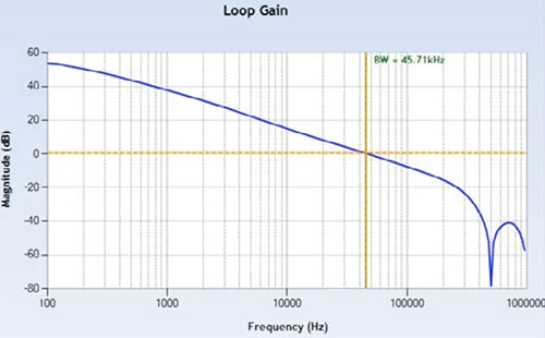
Figure 3(a): Control loop gain for a Linear Technology LTC3829 controller.
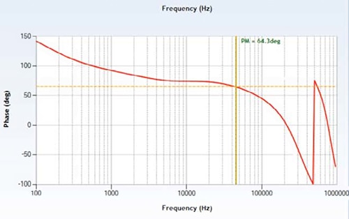
Figure 3(b): Control loop phase for a Linear Technology LTC3829 controller.
From the graphs it can be seen that fc for the LTC3829 is 45 kHz and the phase margin is 64o. The gain margin is close to 20 dB. Such figures make the controller a good basis for a stable yet responsive voltage regulator.
TI makes a wide range of switching supply controller and regulator power modules. Figure 4 shows the frequency response of a reference design from the company based on a TPS23754 controller. The TPS23754 is optimized for an isolated regulator role in Power-over-Ethernet (PoE) powered-device (PD) applications (See the TechZone article “New Generation of PoE Controllers Handles Higher Power With Ease”). Again this is an example of a well-designed switching regulator exhibiting a phase margin of 92o and 25 dB of gain margin.
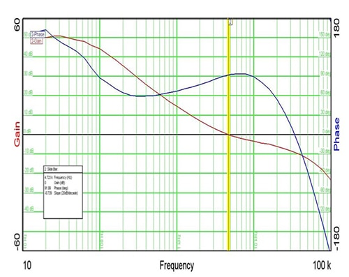
Figure 4: Control loop gain and phase for a TI TPS23754-based power supply reference design for a PoE application.
For its part, Maxim Integrated helpfully includes frequency response Bode plots in its datasheets for many of its switching regulator controllers. The company also supplies devices that integrate not only the inductor, but also the compensation network to ensure the switching regulator is stable and responsive.
The MAX17505, for example, is a high-voltage, synchronous buck regulator with dual integrated MOSFETs and operates over a 4.5 to 60 V input range. It delivers up to 1.7 A over a 0.9 V to 90 percent VIN output voltage range. Figure 5 shows the frequency response of the MAX17505 and indicates an fc of 60.7 kHz and phase margin of 59o.
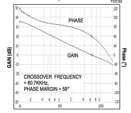
Figure 5: Control loop gain and phase for Maxim MAX17505 switching regulator.
Bench testing required
While in principle the control loop of a switching regulator is simple to understand, its performance in practice is much more difficult to grasp. Even the most expert engineer can take days to compensate a power supply design that looks good on paper but proves to be unstable or exhibits poor dynamic response.
Selecting a controller or regulator module that integrates the majority of a power supply’s components and has been internally compensated by the manufacturer can ease the challenge. However, the addition of external filter components can then alter the frequency response of a module so additional design work will likely be needed. The major component makers offer design software to simulate the frequency response of a proposed design (including external filter components). This shortens the design process, but typically some prototype bench testing will still be required to refine the compensation networks for a well-designed product.
For a deeper analysis of switching regulator control loops and compensator network design, the reader is directed to the Fairchild Semiconductor whitepaper2 by Hangseok Choi, Ph. D.
For more information on the parts mentioned in this article, please click on the links provided to access product pages on the DigiKey website.
References:
- How to Measure the Loop Transfer Function of Power Supplies,” Application Report AN-1889, Texas Instruments, revised April 2013.
- Practical Feedback Loop Design Considerations for Switched Mode Power Supplies,” Hangseok Choi, Ph. D, Fairchild Semiconductor, 2011.
Further Reading
- 1. “Basic Concepts of Linear Regulator and Switching Mode Power Supplies,” Henry J. Zhang, Application Note 140, Linear Technology, October 2013.
免责声明:各个作者和/或论坛参与者在本网站发表的观点、看法和意见不代表 DigiKey 的观点、看法和意见,也不代表 DigiKey 官方政策。


