Ultra-Low-Power MCUs Enable Energy-Harvesting Designs
投稿人:电子产品
2011-06-30
Microcontroller families offer a broad range of on-chip peripherals, featuring nanoampere sleep and microampere active power modes
Energy harvesting holds promise for extending the life of applications with high component reliability but limited battery life. At the heart of any energy harvesting design, ultra-low-power MCUs provide critical data acquisition and conditioning capabilities within tight power budgets. A variety of MCUs combine low power operation with on-chip peripherals that engineers need to meet both application and system-power requirements.
Energy harvesting exploits the generation of tiny amounts of energy from environmental sources on a continuous or near continuous basis. The process converts ambient energy sources into useful power. This approach is particularly promising for applications where power devices are difficult to install and maintain, where cords are too costly or unwieldy, and end points are too numerous or widely scattered to power conventionally. For example, energy harvesting continues to attract growing attention for applications such as tire-pressure monitoring, smart buildings, smart meters and ubiquitous nodes in wireless sensor networks. In some cases, battery-less (or zero-power) operation delivers significant cost benefits. For utility meters, replacing a battery can cost several hundred dollars. In other cases, zero-power operation can enable new classes of applications. For example, in structural health monitoring, battery-operated sensors are simply impractical for buried sensors or those inaccessible due to cost or hazards.
A typical energy harvesting design includes an energy source (such as a solar cell), energy storage (such as a battery), wireless communications subsystem, and application-specific components (such as temperature sensors) and ultra-low-power MCU (see Figure 1).
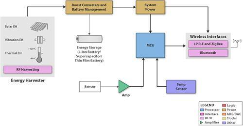
In these designs, energy sources range from as little as 1 nW/cm2 of harvested power from WiFi radio signals to up to 100 mW/cm2 from outdoor light. At these levels, few applications can operate directly from a reasonably sized harvested-energy collector, such as an antenna or solar cell or array. As a result, design of an effective MCU-based energy harvesting application requires careful analysis of power requirements and an ability to adhere strictly to corresponding power budgets.
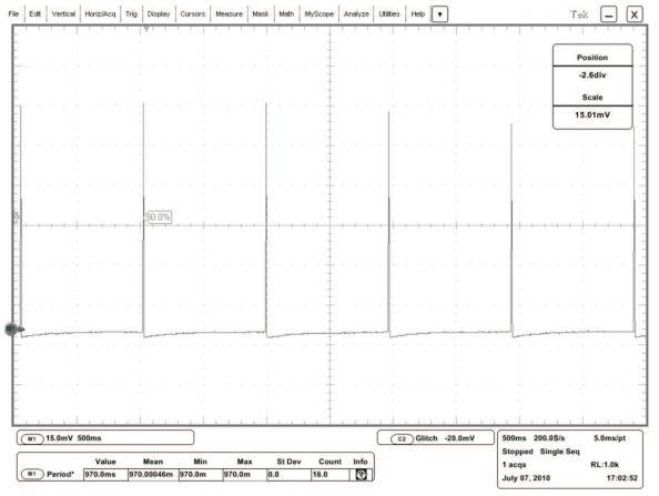
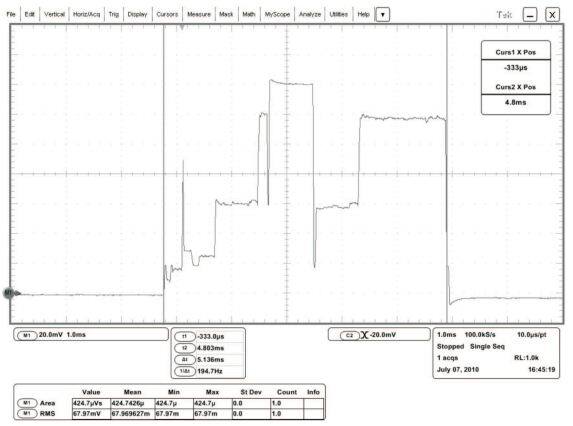
In fact, effective applications of energy harvesting share a set of common characteristics: low data rate and low duty cycle. For example, in one case study of a ZigBee wireless sensor network [ref 1], engineers saw that nodes were in sleep state about 99 percent of the time – active for only 864 milliseconds within a typical one-minute cycle. Although an idealized application might exhibit a simple, regularly repeated current spike (Figure 2), engineers are likely to face more complex current profiles, such as those associated with data conditioning and communications in unreliable or contention-based applications (Figure 2b).
Despite the apparent dominance of sleep-state duration in even simpler applications, an MCU’s power consumption in reaching and maintaining active state largely defines the power budget in these applications. That is, achieving reductions in active current and duty cycle are typically more effective in lowering overall power requirements than achieving low-sleep current states. In fact, engineers will find operational standby current levels well below 1 µA with advanced ultra-low-power MCUs, such as Silicon Labs’ EFM32 family, NXP/Jennic’s JN5148-00 MCU, Microchip’s PIC24F16KA102 MCU, Silicon Labs’ C8051F9xx MCU family and Texas Instruments’ MSP430 MCU family. Ultra-low-power MCUs typically offer multiple levels of standby operation – ranging from limited standby levels in the microampere range to deep-sleep levels in the nanoampere range.
During active mode, these devices exhibit active current levels well under 300 µA/MHz. For example:
- Silicon Labs’ EFM32 32-bit Gecko family features a 180-µA/MHz active run mode with 20-nA sleep current.
- NXP/Jennic’s JN5148-00 32-bit MCU provides a 280-µA/MHz active mode with 100-nA sleep current.
- Microchip’s PIC24F16KA102 16-bit MCU offers 182 µA/MHz in active-run mode with 20-nA sleep current.
- Silicon Labs’ C8051F9xx MCU family features an active current less than 170 µA/MHz with standby current <50 nA.
- Texas Instruments’ MSP430 MCU family offers 160 µA/MHz in active state with standby current <1 µA.
Although active current requirements are critical in ultra-low-power designs, the manner and efficiency when MCUs awaken also affects the required power budget. The increased power required during an extended transition from sleep to active state is wasted power – a serious complication for an application attempting to harvest fractions of milliwatts from the environment (see Figure 3).
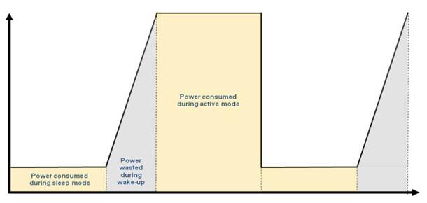
Depending on the application, different sleep-wake schemes may create significantly different duty cycles. Furthermore, although semiconductor manufacturers offering MCUs of this class typically quote wakeup times of 1 to 2 µs, actual wakeup times depend on operating frequency. This requires a balance between increased overall power associated with higher frequency operation and more efficient operation related to faster wakeup times. Consequently, an engineer designing an application based on energy harvesting needs to consider wakeup profiles and their contribution to total power.
For advanced ultra-low-power 16- and 32-bit MCUs, significant differentiation in current offerings lies in the availability of on-chip subsystems, particularly I/O channels, clock management, analog-to-digital converters and wireless communications components (Figure 4). Each off-chip signal excursion consumes additional power, and further wake-up delays become inevitable if the MCU must first activate a quiescent external subsystem. On the other hand, the inclusion of on-chip components that are not required for the application can threaten to push an energy harvesting design over its power budget. As a result, semiconductor manufacturers mix and match their ultra-low-power MCU cores with a broad variety of components needed for specific application areas. Each manufacturer’s MCU family probably includes multiple parts targeting specific ultra-low-power applications, with different combinations of on-chip converters and communications subsystems.
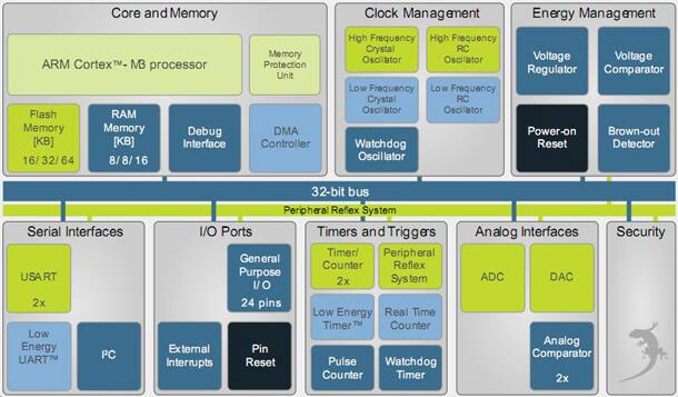
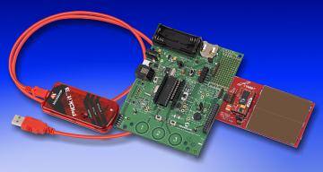
For engineers looking to incorporate energy harvesting techniques in new designs, most ultra-low-power MCU makers offer development kits that combine their flagship MCU with various energy-source transducers and storage devices on a completed board with reference software kits. Two popular development kits include:
- Microchip’s XLP 16-bit Energy Harvesting Development Kit combines its PIC24F16KA102 with Cymbet's EnerChip thin-film storage devices (Figure 5)
- Texas Instruments’ eZ430-RF2500-SEH Solar Energy Harvesting development kit includes TI’s MSP430, Cymbet's thin-film EnerChip devices and a high-efficiency 2.25 x 2.25-inch solar panel optimized for operating indoors under low-intensity fluorescent lights.
免责声明:各个作者和/或论坛参与者在本网站发表的观点、看法和意见不代表 DigiKey 的观点、看法和意见,也不代表 DigiKey 官方政策。




 中国
中国