The Challenges of Choosing Offline LED Driver Topologies
投稿人:Convergence Promotions LLC
2011-11-29
Driver requirement for LED arrays vary widely with overall design criteria. So too will your choice of driver topologies.
When considering LED driver topologies for converting AC input voltage to a constant regulated current source for the LED loads, it is helpful to view LED applications in three general power levels: low-power applications which require less than 20 watts input, for example, light strips, R-lamps, and incandescent lamps; mid-power down light and L-Light applications up to 50 watts input; and high-power signage or street lighting requiring higher than 50 watts input. The designer faces a different mixture of challenges in these three power ranges from cost, space to fit the LED driver, efficiency, design complexity, power factor, mean-time-to-failure, and reliability to name but a few of the challenges. Basic topologies within these three basic power ranges are recommended to satisfy the design challenges.
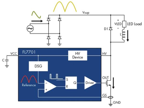
The low-power solutions targeting small lamp sizes require small design volumes to fit the LED driver, consistent light radiation by controlling the current through the LED, efficiency, and low cost. In order to be compliant with Energy Star Program Requirements for Luminaires, the light fixture must have a power factor ≥0.7 for residential applications and ≥0.9 for commercial applications for input power greater than five watts.¹ If isolation from the LED driver is not required, a buck regulator topology is the lowest BOM and therefore a low cost solution to consider. Figure 1 is a non-isolated buck topology example which also includes power factor correction and dimming capability. There is only one magnetic component, which is a simple inductor and a single MOSFET/diode pair for buck power conversion. This topology choice is best selected when the input voltage is larger than the output voltage required from the LED load.
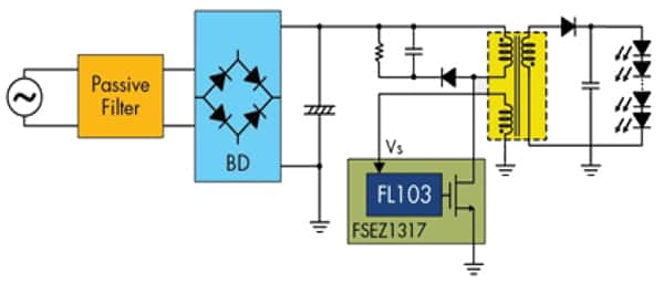
When isolation from the LED driver is required, a good topology choice is the primary-side regulated (PSR) flyback topology. Figure 2 is an example of a PSR flyback LED driver. Reduced cost is achieved by not requiring secondary side feedback, so the topology has a smaller component count to achieving good constant current regulation. The MOSFET can be integrated into the controller to reduce BOM count and reduce the printed wiring board space. The reliability of the PSR flyback is improved without the use of an opto-isolater for secondary feedback.
Discontinuous conduction mode (DCM) is the preferred operating mode for the PSR flyback topology since it allows for better output regulation. The typical waveforms are shown in Figure 3.
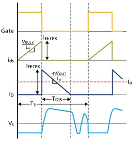
When operating a PSR LED driver in constant voltage regulation mode, during the inductor current discharge time TDIS the sum of the output voltage and diode forward-voltage drop is reflected to the auxiliary winding side. Since the diode forward-voltage drop decreases as the current through the output diode decreases, the auxiliary winding voltage reflects the output voltage at the end of diode conduction time TDIS. By sampling the auxiliary winding voltage at the end of the diode conduction time, the output voltage information is obtained.
When operating in constant current regulation mode, the output current can be estimated using the peak drain current IPEAK and the inductor current discharge time TDIS since the output current is the same as the average of the diode current in steady state. With Fairchild’s innovative TRUECURRENT™ technology, constant current output can be precisely controlled.
Efficiencies for a PSR topology can achieve 85 percent. As an example, consider an 8.4 watt application, the total power loss in the LED driver was measured at 1.32 watts at 85 VAC input. The largest contributors to the loss budget start with the transformer estimated at 0.55 watts loss followed by the snubber (shown in Figure 2 with the series combination diode connected to the parallel resistor and capacitor across the transformer primary winding) at 0.31 watts, the MOSFET at 0.26 watts, and the output rectifier and bridge rectifiers total together 0.20 watts.² The transformer and snubber are generally the worst-case power dissipation components, and it is the leakage inductance from the transformer that requires a snubber to prevent voltage stressing the MOSFET. The printed wiring board and input EMI filter can also become significant sources of power dissipation sources if attention is not paid to these two areas of the design.
The total loss of 1.32 watts may not seem like a significant source of power loss, but in a low-power LED driver the LED loads are close to the driver, so it is the total load power plus driver losses that heat the design. Heat transfer does not have, as an option, forced cooling airflow, so the example cited would have to use a light fixture capable of conducting efficiently 8.4 watts away from the semiconductor and electrical devices in order to maintain reliability. The use of electrolytic capacitors can lower the mean-time-to-failure of the design if the thermal solution is not efficient in removing this power in order to keep component temperatures low.
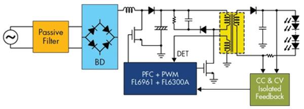
Mid-power solutions still require small design volumes and power factor correction is required. Efficiency and reliability are also important design constraints in this power range. A good topology to use is the single-stage power factor correction flyback topology as shown in Figure 4.
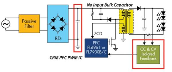
A one-stage design reduces component count and does not require the input bulk capacitor, saving not only volume design space but reducing cost as well. The flyback is controlled for power factor correction and secondary feedback is present. With these mid-power flyback topology designs, efficiencies up to 84 percent can be achieved. Since the topology is a flyback, the transformer and use of a snubber are still the major power dissipation losses in this LED driver design. The higher power level in this mid-power range increases the snubber power loss since snubber loss is proportional to the transformer leakage inductance times the square of the peak current in the MOSFET. In this mid-power design, the transformer increases in size as the peak current in the MOSFET increases.
High-power solutions focus on the best efficiency and reliability at reasonable cost using a low BOM count. A two-stage LED driver is recommended. The first stage is used for power factor correction followed by a DC-DC conversion stage to regulate the constant current output. The first stage can be the same PFC single stage flyback converter as used in the mid-power range. In order to reduce component cost in this two-stage approach, the controller integrates components and features on the first stage.
There are two recommended second stage DC-DC converter choices: a quasi-resonant (QR) flyback for applications under 100 watts or the LLC topology for applications over 100 watts. A flyback achieves reasonable efficiency and is a less complex topology versus the LLC topology choice. The QR topology reduces switching losses associated with the MOSFET output capacitance by reducing the turn-on starting capacitance voltage. The QR topology MOSFET soft switching also reduces EMI. However, for the LLC topology, better efficiency is achieved due to the MOSFET zero voltage switching, enabling a small holdup capacitor to be used. Up to 92 percent efficiency can be achieved in this two-stage approach. Figure 5 and Figure 6 show the QR and LLC topologies. Note that the LLC circuit in Figure 6 uses the leakage and magnetizing inductance of the transformer to create the LLC resonant circuit.

The high-power applications generally use multiple strings of LEDs. Figure 6 shows the use of a secondary controller to balance current through the different LED string loads.
Conclusion
LED driver topologies are dictated primarily by the power level of the array being driven. For low-power luminaires, the primary-side regulated (PSR) flyback topology operating in discontinuous conduction mode (DCM) is recommended, since it can achieve high efficiency and provide good current regulation. For mid-range power requirements a single-stage power factor correction flyback topology provides good efficiency and eliminates the output capacitor. For high-power applications a two-stage LED driver is recommended: a PFC single-stage flyback converter followed by DC-DC converter – either a quasi-resonant (QR) flyback for applications under 100 watts or the LLC topology for applications over 100 watts.
References:
- United States Department of Energy, Energy Star Program Requirements Product Specifications for Luminaires (Light Fixtures) Version 1.0, Effective date: October 1, 2011.
- Fairchild Reference Design RD-L015, 8.4W, FL103 Low Power PSR Flyback.

免责声明:各个作者和/或论坛参与者在本网站发表的观点、看法和意见不代表 DigiKey 的观点、看法和意见,也不代表 DigiKey 官方政策。


 中国
中国