Techniques to Limit Switching DC/DC Converter Inefficiency During Low Loads
投稿人:电子产品
2012-07-03
Stretching the power budget is a common challenge for design engineers developing battery-powered products. Consumers expect more functionality and longer run times from each new product iteration, but, because battery technology improves only very slowly, this is proving increasingly difficult.
Switching DC/DC converters help to improve battery life because their high efficiency helps minimize power consumption. However, efficiency is not constant across the output current range, tailing off markedly at low loads. This is particularly a problem for battery-powered devices that often spend long periods in “standby” or “sleep” modes. Such inefficient operation at low loads results in flawed battery life calculation, shorter product operational times, and disappointed consumers.
This article takes a close look at how the efficiency of switching DC/DC converters varies under load, explains why this happens and points to some products that incorporate technology to mitigate this problem.
Squeezing out the power
Processor chips have improved in performance roughly in harmony with Gordon Moore’s 1965 prediction that the number of transistors on a chip doubles every 24 months. (Actually, the performance has tended to double every 18 months because not only are there more transistors, but they also operate faster.)
Meanwhile, batteries have improved relatively slowly. For example, Lithium ion (Li ion) cells, the mainstay power source for high-demand portable devices such as cell phones and digital cameras, have improved in energy density by only about 7 percent a year (the improvement is mainly due to incremental engineering refinements).
This presents engineers designing portable devices with a dilemma: They want to offer customers faster products with more functionality and brighter screens, yet those same customers demand longer battery life from the enhanced device.
Clever silicon design has resulted in chips running at lower voltages and demanding less power while still offering high performance. However, it is still incumbent on the engineer to ensure that his design makes the most of the advantage endowed by low power consumption silicon by choosing the best power management chips.
A key design decision is the choice of DC/DC converter module to regulate the battery voltage for the sensitive electronics. A poor choice of module might leave consumers thanking the designer for warming their hands on a cold day, but a few hours later cursing him as the display on their smartphone winks out.
Watch the numbers
Like other silicon, DC/DC converters have dramatically improved in performance while prices have dropped. Engineers now have a wide selection of choices when deciding on a power management module for a portable design.
Designers have the option to choose from linear Low Drop Out (LDO) DC/DC converters or switching DC/DC converters. LDOs are inexpensive, compact and relatively easy to design in, but because the conversion efficiency is proportional to input voltage/output voltage, efficiency decreases rapidly with increasing voltage differential. Moreover, as the voltage differential increases, current output is limited.
Figure 1 shows the current output vs. voltage differential for Linear Technology’s LT3070 linear regulator. This is a popular chip for powering microprocessors and FPGAs, among other devices, in portable products. The current limiting as the voltage differential increases can restrict the chip’s usefulness in certain applications.
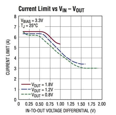
Figure 1: Current limit vs. voltage differential for LT3070 linear converter (Courtesy of Linear Technology.)
In comparison to the linear types, switching DC/DC converters are more expensive, larger, and tricky to design with (see the TechZone article “Conducted and Radiated Emissions Reduction Techniques for Power Modules”). But the big upside–especially for a designer on a tight power budget–is efficiency.
The key reason for this efficient operation is the use of MOSFETs in modern switching converters, replacing the rectifying diode of old designs. In those older products, the diode’s dissipated power equaled the forward voltage drop multiplied by the current, compromising performance.
A MOSFET-based switching converter design is often known as a “synchronous rectifier”. The synchronous rectifier switch is open when the main switch is closed, and vice versa. To prevent cross-conduction (when top and bottom switches are on simultaneously), the switching scheme must be “break-before-make”. Consequently, a diode is still required to conduct during the interval between the opening of the main switch and the closing of the synchronous rectifier switch (the dead time).
When a MOSFET is used as a synchronous switch, the current normally flows in reverse (source to drain), allowing the integrated body diode to conduct current during the dead time. As the synchronous rectifier switch closes, the current flows through the MOSFET channel. Because of the very low-channel resistance for power MOSFETs, the standard forward drop of the rectifying diode can be reduced to just a few millivolts, boosting peak efficiencies to well above 90 percent.
Low load losses
Unfortunately the efficiency curve for a switching converter is not flat; performance at low or high loads is worse than for medium loads. That is particularly a challenge for portable equipment designers because battery-powered devices spend a lot of time in standby or sleep modes to save power when not in use. At these low currents, the switching converter is relatively inefficient and can negate some of the power savings the designer was hoping to achieve in standby or sleep operation.
Figure 2 shows how the efficiency curve of a switching DC/DC converter can be generally divided into three regions. In the high load region, the dominant power losses are due to high conduction losses induced by the load current. In the light load region, power losses result from current ripple-induced conduction losses, and so-called “V–I overlap” switching losses associated with the voltage-current overlap common to a rapid switching cycle. V-I overlap losses are proportional to load current, input voltage, and switching frequency.
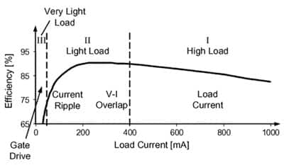
Figure 2: Typical efficiency curve of a DC/DC converter.
The conduction losses caused by the current ripple become dominant because the overlap loss scales down with the load current, while the power dissipated by current ripple normally remains constant. When the DC/DC converter is under very light load, the gate-drive losses, consumed when charging and discharging the gate capacitances of the power transistors during switching transitions, dominate¹.
Fortunately, some modern switching converters employ technology to limit inefficiencies at low and very low loads. One popular technique used to improve things in the low load zone is called “soft switching.” Soft switching eliminates overlap losses by switching the power transistor when either its voltage or its current is zero.
Soft switching, when properly implemented, improves efficiency, lowers electromagnetic interference (EMI), and allows higher frequency operation (allowing the use of smaller magnetic components (see the TechZone article “Design Trade-offs in Integrating an Inductor into a Power Module”).
Zero voltage switching (ZVS), rather than zero current switching, is the preferred technique for high frequency MOSFET applications such as switching DC/DC converters. Figure 3a and b show schematics of the technique for a MOSFET.
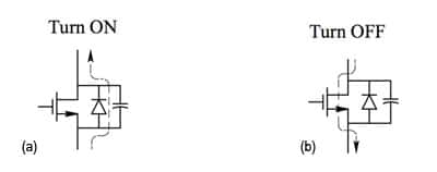
Figure 3: Zero voltage switching in a high frequency MOSFET. (a) Turn on. (b) Turn off.
When turning on, the switch voltage is first brought to zero before the gate voltage is applied, which results in a virtually zero-loss transition. Turning off is a low loss transition and uses a parallel capacitor as a lossless snubber.²Figure 4a and b compares the voltage waveforms for a soft-switched MOSFET compared with a hard switched version. Note the rapid settling of the soft-switched device.
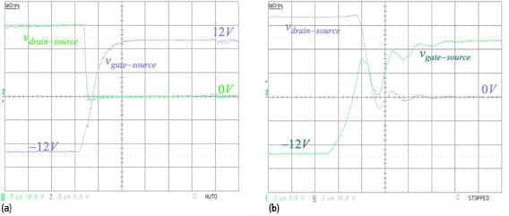
Figure 4: Voltage waveforms for (a) soft-switched and (b) hard-switched MOSFETs.
Improved efficiency comes to commercial chips
There are plenty of soft-switched switching DC/DC converters to choose from. International Rectifier’s iPOWIR iP2005A, for example, is a high-frequency synchronous step-down ("buck") DC/DC converter that the company says is optimized for low power loss and low EMI by the use of soft switching. It can supply a regulated 0.8 to 5.5 V output from a 6.5 to 13.2 V input. Figure 5 shows the efficiency graph for this product at various output voltages.
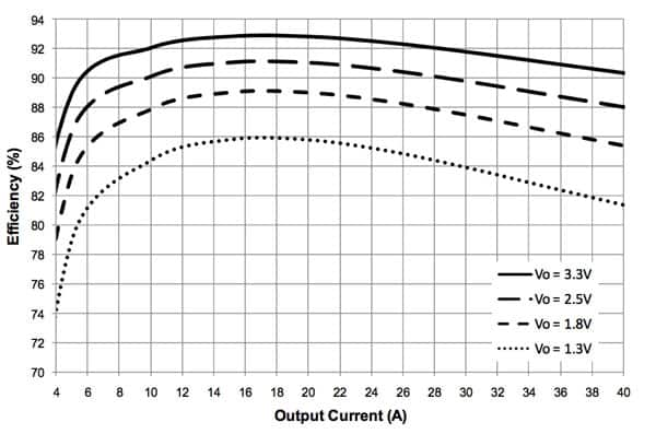
Figure 5: Efficiency curves for iP2005A (VIN = 12 V, Freq = 1 MHz).
In the very low load area, because losses during the switching transitions dominate, one advantageous technique is to either reduce the switching frequency or keep it constant but skip some “on” cycles when the load demand decreases.
In Maxim’s MAX8632, a comparator senses when the current through the inductor reverses and opens the switch, allowing the MOSFET’s body diode to block the reverse current so that the voltage across the inductor goes to zero. A new cycle is then initiated when the output voltage drops below the regulating threshold. While operating in this mode, the switching frequency is proportional to the load current³, so it will vary over time. This so-called discontinuous mode is illustrated in Figure 6.
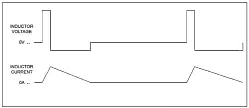
Figure 6: In discontinuous mode the inductor fully discharges and then the inductor voltage rests at zero. (Courtesy of Maxim.)
The discontinuous mode offers improved light load efficiencies, but generates more noise because of the constantly varying switching frequency.
Intersil says its ISL8016 high-efficiency synchronous buck regulator can be configured for discontinuous or forced continuous operation at light load. If EMI considerations are more important than battery life, the chip can run in forced continuous operation to reduce noise during light load conditions. Alternatively, a discontinuous mode provides high efficiency by reducing switching losses at light loads. The ISL8016 can deliver up to 6 A with an output voltage of between 0.6 and 5.5 V from a 2.7 to 5.5 V supply. The chip can be seen in Figure 7.
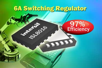
Figure 7: Intersil’s ISL8016 features a discontinuous mode to limit losses at low loads.
In contrast, Texas Instruments’ TPS53353 improves efficiency at low loads by using an “auto-skip” mode. The operating frequency is kept constant, but some switching operations are skipped eliminating the losses normally incurred with every cycle. The TPS53353 synchronous switching buck converter has a peak efficiency of 92 percent and a 0.6 to 5.5 V output. Figure 8 shows how the efficiency at light load is improved by comparing a TPS53353 chip auto-skip mode with one running conventionally.
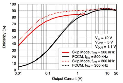
Figure 8: Efficiency vs. output for Texas Instruments TPS53353 in auto-skip mode compared with conventionally operating device.
For its part, National products from Texas Instruments utilizes yet another technique for its LM2651 switching DC/DC converter. This device provides efficient power conversion over a 100:1 load range by entering a hysteretic or sleep mode to maintain efficiency. Figure 9 shows the efficiency vs. load graph for this device. Note that the efficiency still exceeds 80 percent at a 15 mA load.
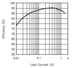
Figure 9: Efficiency vs. load current for National Semiconductor’s LM2651 (VIN = 5 V, VOUT = 3.3 V).
In summary
The biggest challenge of a portable product is managing the power resources while meeting consumer expectations of a big screen, lots of features, and long battery life.
Careful choice of silicon helps, but the designer needs to be aware that switching DC/DC converters that are impressively efficient when the product is working normally can be an insidious drain on batteries when the device is in a low-power mode.
The solution is to look for converter modules that extend battery life by utilizing features such as soft switching, discontinuous operation, and skip modes, as they are more efficient than conventional modules during low load operation.
References:
- “A High Efficiency, Soft Switching DC–DC Converter With Adaptive Current-Ripple Control for Portable Applications,” Siyuan Zhou, Student Member, IEEE, and Gabriel A. Rincón-Mora, Senior Member, IEEE, April 2006.
- “Soft-Switching in DC-DC Converters: Principles, Practical Topologies, Design Techniques, Latest Developments,” Raja Ayyanar, Arizona State University, Ned Mohan, University of Minnesota, Eric Persson, International Rectifier, 2002.
- “DC-DC Converter Tutorial,” Tutorial 2031, Maxim.
免责声明:各个作者和/或论坛参与者在本网站发表的观点、看法和意见不代表 DigiKey 的观点、看法和意见,也不代表 DigiKey 官方政策。


