Structural Defects Undermine LED Luminosity
投稿人:电子产品
2012-04-17
Gradual fading, which is the cause of failure for most LEDs, is primarily due to microcracks in the semiconductor die. These defects are introduced during the complex wafer manufacturing process.
Called threading dislocations, these microcracks multiply over time — more quickly when the LED is exposed to high temperatures — increasing the number of sites where the chip’s charge carriers can recombine without producing light (see the TechZone article “Understanding the Cause of Fading in High Brightness LEDs”).
However, the increase in this so-called “non-radiative recombination” is not the only mechanism that causes LEDs to fail. Threading dislocations also create paths for leakage currents, robbing the LED of yet more valuable charge carriers. The situation gets worse over time as defects multiply, leading to an increased risk of failure from power supply spikes or electrostatic discharge (ESD) events.
This article describes why leakage currents occur and suggests what can be done to slow the process of deterioration during the LED’s operational life, such that the chip delivers on the longevity these solid-state light sources promise.
The perils of leakage current
In an operating LED, charge carriers—electrons and holes—migrate to the device’s p-n junction where there is a good chance they will recombine. Recombination (sometimes) releases light in the visible part of the spectrum. (The previous TechZone article cited above describes in detail the physics behind electroluminescence, the phenomenon behind LED light emission.)
The physics of electroluminescence is governed by quantum mechanics, and quantum mechanics allows electrons and holes to do some weird things. One particular quirk is “tunneling” whereby an electron can surmount a barrier (for example, the energy gap across a p-n junction) that, according to classical physics, would require more energy to cross than the electron possesses. It is a bit like weakly rolling a ball up a steep hill, and, instead of seeing it roll back down the hill, observing the ball burrowing through the hill and appearing on the other side.
In an operating LED, some of this tunneling activity manifests itself as a reverse bias current (“leakage current”) that allows charge carriers to go “against the flow.”
Leakage current, as the name suggests, is not a good thing because the charge carriers that make it up do not contribute to electroluminescence. It is impossible to cheat the laws of physics, so LED makers have accepted that their devices will suffer some leakage current and a slight reduction in efficacy. However, in new devices from major manufacturers the effect is typically negligible.
Nonetheless, all devices are not the same; the initial leakage current of an LED is dependent on the quality of the manufacturing process. And worse yet, it is not constant. The operating conditions (particularly temperature) to which the LED is subject determine how quickly the leakage current increases during operation and how soon it could start to cause problems.
Disappearing charge carriers
It turns out that threading dislocations (vertical microcracks caused by strain generated by the mismatch between the active LED and its substrate during wafer manufacture (Figure 1) are places that exhibit increased probability of tunneling.[1]
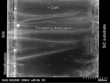
Figure 1: Threading dislocations in LED semiconductor die. (Courtesy of North Carolina State University.)
One group of researchers, for example, has determined that as the threading dislocation density in a sample LED increased from 1.7 x 10⁷ to 2 x 10⁸ per cm² (typical figures for common LED materials such as Indium Gallium Nitride (InGaN) deposited on Sapphire), the LED leakage current increased exponentially.[2] Other scientists determined the leakage current increased 218 times as the threading dislocation density increased from 1.5 x 10⁷ to 2 x 10⁸ per cm² (Figure 2).
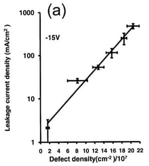
Figure 2: Leakage current increases rapidly as defect density rises.
While the effect on the LED’s luminosity is not quite so dramatic, it is still significant. Both groups noted a 22 percent reduction in luminosity across this threading dislocation range. (Note that this reduction in light output is solely due to leakage current and does not include the additional loss at higher densities due to more sites for non-radiative recombination.)
The researchers explain that the main reason why the reduction in luminosity is not as bad as might be expected is because, while leakage currents are worse at threading dislocations, charge carriers do exhibit a preference for migrating to Indium-rich “wells” in the crystal away from dislocations where they can happily recombine and emit a photon. The effect partially nullifies the loss of charge carriers down the microcracks.
New materials hold promise
Much of the current focus by premium vendors such as OSRAM, Cree, and Seoul Semiconductor is on enhanced manufacturing techniques designed to limit the number of threading dislocations in new wafers. That is not an easy business, because the active LED semiconductor InGaN and the typical substrate materials have poorly matched crystal structures.
A careful choice of vendor can make a big difference in the initial brightness and longevity of the high brightness LED. For example, some vendors have turned to Silicon Carbide (SiC) as it promises to improve LED quality by reducing the density of threading defects during manufacture (again, see “Understanding the Cause of Fading in High-Brightness LEDs”). Recently, for instance, Cree introduced a range of high brightness LEDs, the XLamp XB-D family, built on SiC technology. OSRAM uses the material for some of the products in its TOPLED range.
Other developments include dispensing with a SiC substrate altogether and manufacturing the active LED from bulk InGaN. Because there is no crystal lattice mismatch between two different materials, threading dislocation density is dramatically lowered. The downside is that the wafers currently cost about four times as much as those built using conventional materials, so manufacturers are understandably reluctant to use them for the price-sensitive mainstream lighting market.[3]
Careful choice of LEDs when new is only part of the challenge. The way a design engineer uses an LED influences how threading dislocation multiply over time, potentially increasing leakage current and accelerating the device’s eventual demise.
Investigating reverse bias
LEDs are, as the name states, a form of diode. These devices have an interesting voltage current relationship (Figure 3). In normal operation, a constant forward voltage of sufficient magnitude (>Vd) is applied (typically with the LED in series with a resistor), such that the device is operating in its conduction region. It is important that the forward voltage is carefully controlled, because beyond the conduction voltage, small fluctuations cause dramatic changes in the forward current, light intensity, and power dissipation.
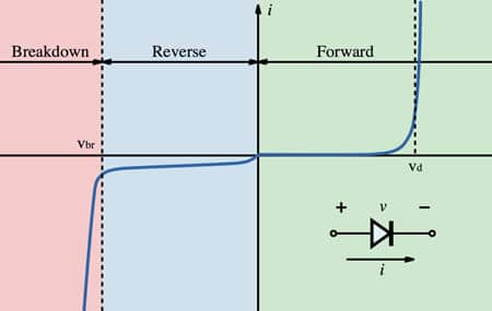
Figure 3: Diode voltage vs. current characteristic.
Figure 4 shows detail of the forward voltage vs. forward current for a commercial high brightness LED, in this case a 60 lm/W Seoul Semiconductor device. From the graph, it can be seen that conduction starts at around 2.5 V. The manufacturer recommends operating with a typical forward voltage of 3.6 V.
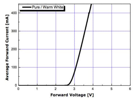
Figure 4: Forward voltage vs. forward current for commercial high brightness LED. (Courtesy of Seoul Semiconductor.)
For the purposes of this article, the main area of interest is what happens under reverse bias conditions. (Note that the scale on the left side of Figure 3 is magnified compared to the right side, which is why there is a jump in the line around the origin.) Initially, large changes in the reverse bias voltage have little effect on the reverse bias current; at a critical voltage (dubbed the breakdown voltage, or Vbr), further small changes in voltage cause a dramatic escalation in reverse bias current. However, unlike in the forward bias conduction region, operation in the breakdown region will be short-lived because the device will be damaged and will likely soon fail catastrophically.
Many manufacturers do not specify the breakdown voltage in the data sheet because, in normal use, they are not expecting the LED to operate under reverse bias conditions. There are some exceptions however, notably Cree. For its XLamp ML-B family, for example, the company notes the maximum reverse voltage is 5 V.
Nonetheless, manufacturers of LEDs test their new devices to establish the leakage current and breakdown voltage. Devices with high values of the former and low of the latter are scrapped, such that in supplied devices, the tolerance of the LED to reverse bias is as wide as possible.
Things change over time, however, because threading dislocations multiply even during an LED’s normal operation (and escalate dramatically if the chip is overheated). As we have seen, more threading dislocations increase both leakage currents and non-radiative recombinations. Eventually, luminosity drops to a point where, it is below 70 percent of the device’s output when new and “failure” occurs (see TechZone article “Determining LED Rated Life: A Tricky Challenge”).
While fading is the most common cause of LED failure it is not the only way a chip suffering from an excess of threading dislocations can die. The appearance of new defects over time alters the physical characteristics of a chip compared to a new device, causing the breakdown voltage to decrease. Coupled with the increase in leakage current, this has the effect of reducing the threshold between safe operation and catastrophic failure due to exposure to high reverse voltage.
It is a very rare occurrence for the leakage current to build up to a point that the reverse bias breakdown voltage is exceeded in normal operation, but a weakened device, subject to reverse bias from a voltage spike in the power supply or an electrostatic discharge (ESD), could be pushed over the edge to a premature demise.[4]
Summary and recommendations
Modern LEDs are impressive devices, but they have an Achilles Heel. Unavoidable tiny structural defects created during manufacture provide paths for charge carriers to escape without contributing to light output. These defects multiply over time, further reducing luminosity and, in the worst cases, causing premature failure.
LED manufacturers are experimenting with alternative manufacturing techniques and materials, and some have released products with fewer threading dislocations when new, but engineers are advised to incorporate adequate precautions into their designs to limit the inevitable effects of defects.
First, it is a good idea for the engineer to buy from a reputable distributor who stocks parts from the leading manufacturers. Second, the LED should be operated at the forward voltage recommended by the supplier using a good quality LED driver power supply from manufacturers such as Fairchild Semiconductor and Diodes, Inc. Third, the engineer should protect the chip from mechanical stress and exposure to ESD events. And fourth, it should come as no surprise for the engineer to learn that the LED should be adequately cooled.
References:
- “Influence of defects on electrical and optical characteristics of GaN/InGaN-based light-emitting diodes,” X. A. Cao et al, GE Research Center, Niskayuna, NY.
- “Effect of defects on the electrical/optical performance of gallium nitride based junction devices,” Ferdous, Mohammad Shahriar, Ph.D., The University of New Mexico, 2008.
- “SiC, sapphire and GaN materials status into Opto and RF businesses,” Dr. P Roussel, Yole Development, Lyon, France.
- “Damage of light-emitting diodes induced by high reverse-bias stress,” N. C. Chen et al, Institute of Electro-Optical Engineering, Department of Electronic Engineering, Chang Gang University, Taiwan, ROC.
免责声明:各个作者和/或论坛参与者在本网站发表的观点、看法和意见不代表 DigiKey 的观点、看法和意见,也不代表 DigiKey 官方政策。


