Simple Circuit to Generate Plus and Minus Supplies Using a Boost Regulator
投稿人:DigiKey
2012-08-28
Combining the operation of a boost regulator and a negative voltage converter can generate a negative supply from a single low-voltage supply. The circuit in Figure 1 shows a standard application circuit for a +20 V supply along with two op amps, two diodes and two capacitors to generate the – 20 V supply. This article will discuss the basic operation of a boost converter to generate a larger positive supply voltage. Equations are derived to determine the minimum inductor value to maintain a safe peak inductor current, and a maximum inductor value to maintain continuous conduction mode (CCM) operation. The article will then discuss the generation of a negative supply and the restrictions of the design.
Understanding the boost topology
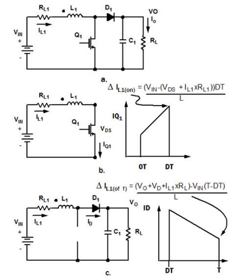
Before we add the additional circuitry to generate the negative supply, it is important to understand how the boost convertor produces an output voltage that is always greater than the input voltage. In order to do this, we analyze the boost circuits in Figure 1 and the current waveforms in Figure 2. For this analysis, we account for all the losses in the charging and discharging loops in our equations. This should help to give a complete understanding of the circuit.
However, the output voltage is not dependent upon any losses in the circuit. This is because all the losses are inside the circuit’s feedback loop of the ISL97701—which we will use as an example here—and are automatically accounted for. The output voltage is defined from the feedback resistor network shown in Figure 1 and calculated in Equation 1, where VrefFB is the internal reference voltage of the ISL97701.
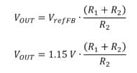
Equation 1
Positive supply
Figure 1a shows the basic boost converter circuit. During one switching cycle, the transistor Q1 turns on and turns off. During the time Q1 is on, the inductor L1 is placed in series with the VIN supply through the ISL97701’s integrated boost FET (Q1). The diode D1 is reverse biased and the circuit reduces to that shown in Figure 1b. The voltage across the boost inductor (L1) is equal to VIN – (VDS + IL1 x RL1) and the current ramps up linearly in inductor L1 to a peak value at time DT. The peak inductor current (ΔIL1) is calculated in Equation 3 and shown graphically in Figure 1b. Any load requirements during this phase are supplied by the output capacitor C1.

Equation 2

Equation 3
When Q1 turns off, because the current in an inductor cannot change instantaneously, the voltage in L1 reverses and the circuit becomes that shown in Figure 1c. Now the no-dot end of L1 is positive with respect to the dot end and D1 becomes forward biased. Because the dot end is at VIN, L1 delivers its stored energy to C1 and charges it up to a higher voltage than VIN. This energy supplies the load current and replenishes the charge drained away from C1. During this time, energy is also supplied to the load from VIN. The voltage applied to the dot end of the inductor is (VIN – IL1 x RL1). The voltage applied to the no-dot end of L1 is now the output voltage (VO) plus the diode forward voltage (VD). The voltage across the inductor during the off-state is ((VO + VD1 + IL1 x RL1) – VIN). The inductor current during the off-time of the switch (T-DT) is calculated in Equation 4 and shown graphically in Figure 1c.

Equation 4
In steady-state conditions, the current increases during the on-time of the switch and decreases during the off-time of the switch (Figure 2). Both on-time and off-time currents are equal to prevent the inductor core from saturating. Setting both currents equal to each other and solving for VO results in the continuous conduction mode boost voltage shown in Equation 5.

Equation 5
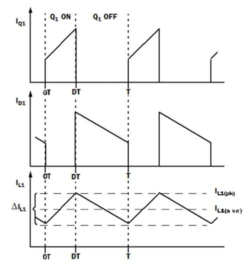
The duty cycle (D) in Equation 5 is determined by setting the losses in Equation 5 (IL1 x RL1, VD1, VDS) to zero because they are within the feedback loop of the ISL97701. The ISL97701 varies the duty cycle continuously to keep VO constant, regardless of the conduction losses as a function of load current. With the losses set to zero, Equation 5 reduces to Equation 6. This results in the value for the duty cycle shown in Equation 7.

Equation 6

Equation 7
Inductor selection
The inductor selection determines the output ripple voltage, transient response, output current capability and efficiency. Its selection depends on the input voltage, peak inductor current, output voltage, switching frequency and maximum output current. When choosing an inductor, make sure the saturation current of the inductor is greater than the IPEAK of the circuit. Likewise, the transistor should be able to handle peak current greater than IPEAK. The peak inductor current is shown in Figure 3 and can be calculated using Equation 8.
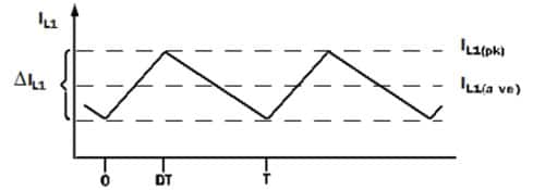
From Figure 3, we can see that the peak inductor current IL1 is equal to the average inductor current IL1 plus one half the Δ IL1 current, as shown in Equation 8.

Equation 8
The average power IN is equal to the average power OUT divided by the efficiency of the circuit, as shown in Equation 9.

Equation 9
Where Eff is equal to the efficiency of the ISL97701 boost regulator. Therefore, the average inductor current is equal to the output current multiplied by the gain of the boost regulator as shown in Equation 10.

Equation 10
ΔIL1 was defined in Equation 3 and the duty cycle (D) in Equation 7. Substituting Equation 7 into Equation 3 and adding it to Equation 10 results in Equation 11. Equation 11 gives the inductor’s peak current in terms of input voltage, output voltage, switching frequency, and maximum output current (again, the losses due to VDS and IL1 x RL1 are not included because they are inside the feedback loop of the ISL97701).

Equation 11
By rearranging the terms in Equation 11, we can solve for the inductor value using Equation 12.

Equation 12
Equation 12 is useful for determining the minimum value of L that the circuit can handle without exceeding the peak current through the inductor, and therefore the switch Q1. The maximum peak current (IPEAK) allowed through Q1 for safe operation is given in the electrical table as 1.2 A.
Minimum inductor value design example
Given: VIN = 5 V, VO = 20 V, IO = 50 mA, IPK = 1.2 A, freq = 1 MHz, Eff = 0.85 (Efficiency of 85% from Figure 3 in the ISL97701 data sheet).
Equation 12 gives us the boundary condition for the smallest inductor we can have to ensure the peak current through Q1 is less than the max limit of 1.2 A. Plugging all these numbers into Equation 12 (see Equation 13) results in the minimum inductor value for the given conditions to be 1.94 μH.

Equation 13
Maintaining CCM design example
For maximum efficiency, the boost converter needs to be operated in continuous conduction mode (CCM). To maintain continuous conduction mode operation of the boost regulator, the value of IL1 needs to be greater than or equal to ΔIL1/2 (Equation 14).

Equation 14
Rearranging terms and solving for L results in Equation 15.

Equation 15
To maintain continuous conduction mode operation for the given circuit design conditions above, the value of L has to be greater than 7.96 μH (Equation 16).

Equation 16
It should be noted that when there is a light load, the circuit can slip into discontinuous conduction mode, where the inductor becomes fully discharged of its current each cycle. This operation will reduce the overall efficiency of the supply. Using Equation 15 and making the value of the inductor large enough for a given minimum output current will ensure continuous conduction mode operation.
Output capacitor
Low ESR capacitors should be used to minimize the output voltage ripple. Multilayer ceramic capacitors (X5R and X7R) are preferred for the output capacitors because of their lower ESR and small packages. Tantalum capacitors with higher ESR can also be used. The output ripple can be calculated in Equation 17:

Equation 17
For noise sensitive applications, a 0.1 µF placed in parallel with the larger output capacitor is recommended to reduce the switching noise.
Negative supply
The operation of the negative supply is best understood by considering Figure 5. We will start our analysis under steady state conditions (the inductor operating in continuous conduction mode and C1 is equal to the voltage calculated in Equation 1).
When Q1 turns off, the inductor voltage flies up turning on D1 and D3. Diode D2 is blocking current flow from C3. The inductor current now charges both capacitors C1 and C2 with the polarity shown in Figure 5. The voltage on C2 is equal to the voltage on C1 plus the forward voltage drop of D1.
When Q1 turns on, Diodes D1 and D3 are blocking and capacitor C2 is now in parallel with capacitor C3 through D2 (which is now on), reference Figure 4. This connection results in a negative voltage being transferred on to C3. The voltage transferred to C3 is equal to the voltage on C1 as shown in Figure 4 and Equation 18.
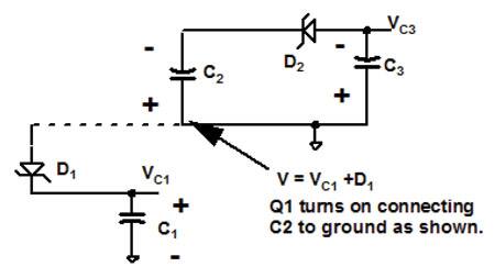

Equation 18
The efficiency of the charge transfer between the two capacitors is related to the energy lost during this process. ENERGY IS LOST ONLY IN THE TRANSFER OF CHARGE BETWEEN CAPACITORS IF A CHANGE IN VOLTAGE OCCURS. The energy lost is defined in Equation 19:

Equation 19
Where V1 and V2 are the voltages on C2 during the charging and transfer cycles. If the impedances of C2 and C3 are relatively high at the 1MHz frequency compared to the value of RL, there will be substantial difference in the voltages V1 and V2. Therefore it is not only desirable to make C3 as large as possible to eliminate output voltage ripple, but also to employ a correspondingly large value for C2 in order to achieve maximum operation efficiency.
Output voltage regulation using op amps
The final output voltage regulation is accomplished using the ISL28208 Dual Opamp. The voltage developed by the boost converter powers the amplifiers and the output voltage is calculated using Equations 20 and 21.

Equation 20

Equation 21
Restriction on design
For reasonable voltage regulation of the negative supply voltage, the negative supply current needs to be less than or equal to the positive supply current. This is because the control loop for output voltage regulation is around the positive supply voltage only.

Equation 22
The ISL97701 is optimized to work best for a small range of inductors. The slope compensation ramp generator, inside the ISL97701, is optimized for inductor values between the range of 4.7 μH to 15 μH and output currents between 25 mA and 125 mA. The circuit will work perfectly fine outside these ranges, as long as the maximum IPEAK current is not exceeded (Equation 11). The only drawback will be a reduction in the efficiency of the circuit. The percent efficiency could drop from the 80s to the 60s as the operation goes from continuous conduction mode to discontinuous conduction mode. Reference the ISL97701 data sheet for additional information on performance.
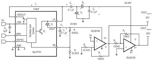
Figure 5: Standard application circuit for a +20 V supply to generate a – 20 V supply.

免责声明:各个作者和/或论坛参与者在本网站发表的观点、看法和意见不代表 DigiKey 的观点、看法和意见,也不代表 DigiKey 官方政策。


 中国
中国