Replacing the Candle in the Candelabra
投稿人:DigiKey
2013-07-23
Two compact, efficient bulb replacement design ideas
LED lamps are now displayed prominently in retail stores as plug-in replacements for standard incandescent lamps. Fitting the protection and constant-current drive electronics required by LEDs within the neck of standard size bulbs is a squeeze, especially for lights using a T8 tube or a compact, Edison-screw based design. In applications like these, space for drive electronics is extremely small and limits both size and number of components that can be used. The lack of space also exacerbates the problem of thermal management. To make matters worse, the LED load is positioned so it is in intimate thermal contact with the power supply. To avoid overheating and consequent failure, the LED driver must operate at the highest possible efficiency.
Stringent regulations
As well as delivering a stable constant-current output, the LED driver (power supply), must comply with increasingly stringent regulations covering power factor and harmonic distortion of the current drawn by the supply.1 Many LED driver solutions use a two-stage approach featuring a boost PFC stage followed by a constant-current driver, often a flyback converter. The boost PFC stage typically achieves a maximum efficiency of perhaps 95 percent and the constant-current driver approximately 90 percent, resulting in an overall efficiency of 85 percent.
This approach requires an inductor, two power switches, and two controllers, – a lot of components to fit into a tiny lamp housing. The PFC stage and the flyback converters are both performing a similar function of switching current flow on and off, or shaping the input and output current, respectively. If the two switching activities could be combined into a single stage, fewer components would be required, and much higher efficiency could be achieved with only one driver circuit and one switching stage.

Figure 1: Single stage LED driver using a combined PFC and CC converter.
Such a circuit is shown in Figure 2 - a single stage, combined PFC and constant current driver, using a LinkSwitch™-PH IC produced by Power Integrations Inc.2 The monolithic device incorporates a 725 V power MOSFET together with integrated control and protection circuitry.

Figure 2: Single stage combined PFC and CC converter Using LinkSwitch-PH (Source: Power Integrations).
Controlling PFC and constant current
The controller combines a proprietary power-factor correction technique with a primary-side-control continuous-conduction mode PWM switching power stage. By combining this control approach along with a monolithic power MOSFET and associated drive circuitry inside a single integrated circuit, it is possible to dramatically reduce component count for the LED driver.
Using the LinkSwitch-PH IC and the circuit shown in Figure 2, it is possible to achieve a conversion efficiency of greater than 90 percent for a 15 W LED driver (equivalent to a 60 W incandescent bulb) in a circuit that requires fewer components than an equivalent two-stage approach. Because input current is shaped directly by the power switch, an input bulk capacitor is not required. The LED driver does not employ electrolytic bulk capacitors, which have short lifetimes in the elevated ambient temperatures seen in LED lamps, which can cause problems for two-stage solutions.
Non-isolated Solutions for Lowest Cost
While isolated flyback converters are extremely effective, they have some limitations with respect to efficiency, size, and cost. Switching losses in the power transformer reduce overall efficiency, while electrical isolation clearance space can occupy upwards of 15 percent of the total available board area in an 8 W converter. The cost of the magnetics is higher as the transformer must meet high-voltage isolation requirements and more expensive construction.
A simpler and potentially lower cost approach, at least for power levels up to 30 watts, is to make the power supply non-isolated and use the bulb enclosure as the safety isolation. This permits the use of simple buck/buck-boost converters which are more efficient (no transformer losses) and use lower cost magnetics (inductors). It is still possible to employ the single stage combined PFC plus CC conversion approach using devices from the LinkSwitch-PH family already described, and the LinkSwitch™-PL family from Power Integrations. These devices can be configured as very efficient buck converters for low-voltage outputs, deliver high PF with low THD, and realize the savings inherent from high-integration and simple buck architecture. This approach works very well for many designs and especially for high-line applications (176 VAC to 264 VAC).
High efficiency is obtained using the highest possible LED string voltage, but, especially in low-line (90 VAC to 132 VAC) applications, this approach reveals a limitation of buck converters. If the output string voltage is too high, buck converters are not able to deliver solutions with low enough THD to meet EN61000-3-2 (C/D) or reach typical ATHD limits of 20 percent. Low THD is achieved by creating a current waveform that is closely matched in shape to the sine wave of the voltage waveform. Buck converters can only pass current to the output stage when the input voltage (rectified sine wave) exceeds that of the output stage. Thus, for a part of each AC line half-cycle, as voltage rises from zero (and as voltage approaches zero), no power-factor correction can occur and THD is reduced. For high output-voltage, (exceeding perhaps 35 VDC in a low-line application), the conduction angle is so short that the converter is no longer able to generate a current waveform that meets EN61000-3-2C/D harmonic current limits.
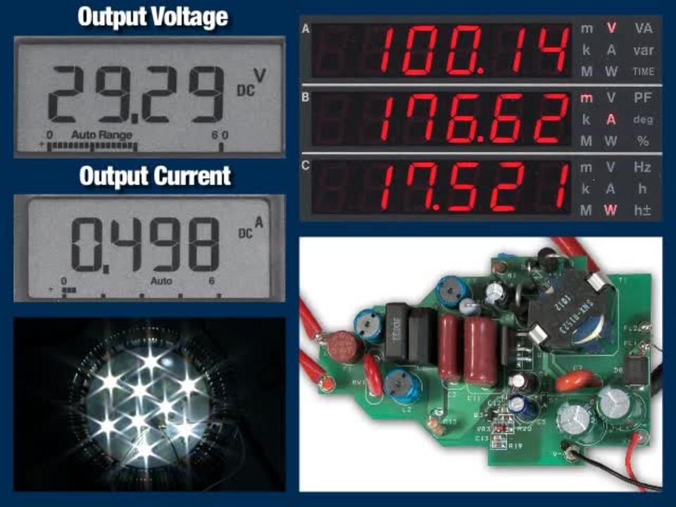
For many non-isolated LED drivers in high-efficiency applications, a buck-boost converter approach is used. An inherent advantage of buck-boost is that it continuously draws power from the AC-input regardless of output voltage level, enabling the input current to be near sinusoidal. Two examples demonstrate the efficacy and elegance of this approach. The first is a long-string LED driver designed to fit within a T8 tube lamp. The circuit is capable of driving a 100 V LED string, yet achieves an efficiency of over 91 percent, power factor greater than 0.9, and THD of over 25 percent. The second design uses the bare minimum of components and is intended to fit within the small B10 lamp enclosure.

Figure 3: Schematic for a 25 W buck-boost LED driver using LNK409EG (Source: Power Integrations).
Figure 3 is a complete non-isolated 25 W power factor corrected LED driver circuit employing buck-boost topology.3 It provides a 250 mA constant-current output at a nominal 100 V from a 180-265 VAC input.
The physical design is remarkable, as shown in Figures 4 and 5. The circuit board is only 19.5 mm wide and 10 mm high.

Figure 4: Populated circuit board (Source: Power Integrations).

Figure 5: LED driver mounted in a T8 tube (Source: Power Integrations).
The buck-boost power circuit is composed of U1, output diode D6, output capacitors C5 and C7, and output inductors T1 and T2. Two inductors are used due to space constraints within the tube. T1 and T2 together provide the required buck-boost inductance, and the bias winding in T1 provides the supply current to U1 and feedback for the disconnected load/overvoltage shutdown function.
No current sense
LinkSwitch-PH ICs provide a highly accurate output constant-current control without the need for a current sense resistor in series with the load. R7-R10, Q1, C6, and D5 comprise a voltage-to-current converter network that delivers a control current to the FEEDBACK (FB) pin proportional to the output voltage. Diode D1 and C3 detect the peak AC line voltage. The voltage across C3, along with R3 and R4, sets the input current fed into the VOLTAGE MONITOR (V) pin. This current is used by U1 to control line under-voltage (UV), overvoltage (OV), and feed-forward current.
The internal control engine within LinkSwitch-PH devices combines the FEEDBACK pin current, the VOLTAGE MONITOR pin current, and the drain current information to provide a constant output current over a 1.5:1 output voltage variation (LED string voltage variation of ±25 percent), at a fixed line input voltage. The constant-current control engine compensates for inductance tolerance, as well as input and output variations.
A low EMI signature is the result of the continuous conduction mode PFC function of LinkSwitch-PH together with frequency jitter. This EMI filtering is simple and small enough to fit within the confines of the T8 tube.
Candelabra
The design goals of the application in the second example were high efficiency and small size, making the driver suitable to fit into candelabra and B10 size lamps.

Figure 6: 4.5 W buck-boost power supply using LNK458KG (Source: Power Integrations).
Figure 6 shows a 4.5 W Power Factor Corrected LED Driver (Non-Isolated Buck-Boost), this time using Power Integrations’ LinkSwitch-PL LNK458KG.4 LinkSwitch-PL5 ICs are very similar to the LinkSwitch-PH devices discussed earlier. They are optimized for lower power, non-isolated applications (up to 16 W) and are supplied in a package with only four connections. The control algorithm uses direct LED current sensing and can support flicker free TRIAC dimming with minimal external components.
The circuit shown in Figure 6 delivers a 90 mA constant-current output over 42 – 56 V from a 85 –135
VAC input. Despite the very small component count, the LED driver achieves over 86 percent efficiency, a PF greater than 0.95 and THD over 15 percent at 115 VAC.

Figure 7: Populated circuit board (Source: Power Integrations).
The populated circuit board in Figure 7 is only 16 mm wide and 28 mm long.
Design choices
A number of important design choices were made to minimize component count and maximize efficiency. The design is optimized to operate over the low AC input voltage range (85 –135 VAC and 47– 63 Hz). In use, the driver is enclosed in a sealed casing together with the LED load. The non-isolated output relies on the casing to provide protection for the user and, if the LED output fails open-circuit, the driver will shut down to prevent overvoltage occurring.
At the input to the circuit, EMI filtering is performed by the 2-π filter network comprised of Capacitors C1, C2, C3, and differential choke L1 and L2. The input filter plus the frequency jittering feature of LinkSwitch-PL devices allow for compliance with Class B emission limits. The limited total capacitance maintains high power factor.
The buck-boost power train is composed of U1 (power switch + control), D2 (freewheeling diode), C7 (output capacitor), and L3 (inductor). Diode D1 is used to prevent negative voltage appearing across the drain-source of U1, especially near the zero crossing of the input voltage. The bypass capacitor C4 provides the internal supply for the device when the power MOSFET is on. The output current feedback is sensed on the voltage drop across R3, and then filtered by a low pass filter (R4 and C5) to keep the LinkSwitch-PL IC operating point, such that the average FEEDBACK (FB) pin voltage is 290 mV in steady-state operation.
The output current operating point can be set merely by adjusting the values of R3 and R5. By changing R3 to 12.7 Ω and R5 to 13 Ω the circuit will deliver 45 mA at 96 V nominal output.
References
- IEC 61000-3-2 Class C harmonics
- LNK403-409EG/413-419EG LinkSwitch-PH Family LED Driver IC, Single-Stage PFC, Primary- Side Constant Current Control and TRIAC Dimming/Non-Dimming Device Options
- DER-278 No Electrolytic Capacitor, High Efficiency (≥90%), High Power Factor (>0.9) 15 W LED Driver Using LinkSwitch-PH LNK407EG. www.powerint.com April 2011
- DER-297 4.5 W Power Factor Corrected LED Driver (Non-Isolated Buck Boost) Using LinkSwitch-PL LNK458KG www.powerint.com October 2011
- LNK454/456-458/460 LinkSwitch-PL Family. LED Driver IC with TRIAC Dimming, Single-Stage PFC and Constant Current Control for Non-Isolated Applications. www.powerint.com November 2010
免责声明:各个作者和/或论坛参与者在本网站发表的观点、看法和意见不代表 DigiKey 的观点、看法和意见,也不代表 DigiKey 官方政策。