Protecting MCU I/O Lines from ESD and Other Transients
投稿人:电子产品
2014-06-11
To do something useful, a microcontroller (MCU) must be connected to other devices. This connection is made through input/output (I/O) pins. More times than not, these days pins are multifunctional and can connect to A/Ds, D/As, linear functions (such as op amps and comparators), voltage references, and more. So for the design engineer, protecting these I/Os against potentially damaging static charges and other similar threats is of high importance.
In establishing proper protection for an MCU, engineers are finding that characteristics they have depended on for years have suddenly become less effective and they are forced to revisit problems of the past. Why? Principally, as a result of market pressure to reduce the cost of their products, semiconductor manufacturers have combined a higher level of integration with continued shrinking of process geometry, making die sizes smaller. As a result, implementing the necessary transient immunity protection to prevent malfunction due to transients on power and signal lines has become increasingly difficult.
When geometries and IC feature sizes were larger, I/O pads had a lot of area for meaty drivers and good protection against ESD-induced damage. In the effort to improve yield, smaller die and pads are used, which, just by their nature, are less able to take a hit to protect a micro. As a rule of thumb, an electrostatic charge will always arc through the shortest possible path, and delicate micro I/O lines lead to more static discharge hits getting through.
This article looks at the different levels of MCU immunity to electrical fast transients (EFT), electrostatic discharge (ESD), and other events of short duration and suggests practical hardware and design techniques that can provide cost-effective ways of protecting microcontroller I/O lines. All parts, data sheets, tutorials, and development systems referenced here can be found online at DigiKey's website.
Immunity performance
One can categorize transient threats into three major types: electrostatic discharge (ESD), electrical fast transient (EFT), and surge transients. To ensure circuit robustness against these transients, the International Electrotechnical Commission (IEC) has specified a series of transient immunity tests in its IEC61000-4 family of electromagnetic compatibility (EMC) standards: IEC61000-4-2 covers ESD immunity (as applied to handheld devices, such as portable phones and computers), IEC61000-4-4 does the same for EFT immunity and IEC61000-4-5 handles surge immunity (lightning and industrial surges).
Immunity performance for integrated circuits is further classified into one of four categories as specified in an IEC document (IEC 62132-1).¹ Class A performance is defined as normal performance within the specification limit during application of the transient. Class B performance is temporary degradation or loss of function or performance which is self-recoverable after the transient is removed. Class C performance is defined as temporary degradation or loss of function or performance that requires operator intervention or system reset after the transient is removed. Class D performance is permanent degradation or loss of function that is not recoverable due to damage or loss of data.
Various standards groups have analyzed transient voltage occurrences using standardized testing and monitoring and have agreed upon several levels of protection needed based on characteristics of conditions (Table 1). Taken into account are the characteristics and limitations of the types of drivers, I/O transistors, and semiconductors used for these applications (Table 2).
| Voltage | Current | Rise-Time | Duration | |
| Lighting | 25 kV | 20 kA | 10 μs | 1 ms |
| Switching | 600 V | 500 A | 50 μs | 500 ms |
| EMP | 1 kV | 10 A | 20 ns | 1 ms |
| ESD | 15 kV | 30 A | <1 ns | 100 ns |
Table 1: Key characteristics of several transient types.
| Device Type | Vulnerability (volts) |
| VMOS | 30-1800 |
| MOSFET | 100-200 |
| GaAsFET | 100-300 |
| EPROM | 100 |
| JFET | 140-7000 |
| CMOS | 250-3000 |
| Schottky Diodes | 300-2500 |
| Bipolar Transistors | 380-7000 |
| SCR | 680-1000 |
Table 2: Device interface technology susceptibility characteristics.
Among other factors, an MCU's performance when impacted by an ESD or EFT event is affected by its process technology, the IC's package, printed circuit board (PCB), software running on the MCU, and the characteristics of the ESD or EFT event.
Texas Instruments microcontrollers like the TMS320F28035PAGT will comply with IEC standards, but can still get zapped with large bursts of charge, especially when interfacing to cabling and connectors for applications such as SD/MMC cards, USB, IEE1394, and Gigabit Ethernet.
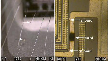
Automotive applications can also introduce high-voltage discharges. Freescale Semiconductor MCUs such as the MCF5329CVM240, leverage the extensive testing and failure analysis done by the company and its predecessor (Motorola) during the evolution of hardened processors for military and aerospace. They have isolated the two failure mechanisms for electrical overstress (EOS) as a function of the total energy applied to the pin. In one case, bond wires can be fused, and if the bond wire can deliver the charge to the internal I/O pad, fuse die metallization can take place (Figure 1).

Figure 1: If allowed to get through, as little as 1 A can cause die wire fusing and substrate metallization even with internal protection.
Microcontroller makers like STMicroelectronics use a variety of their own test systems (like Fast Transient Burst [FTB] testers) to test MCUs such as the STM32F429IIT6, which features a high-performance ARM® 32-bit Cortex™-M4 processing backbone that can interface to several external I/O structures that can be sensitive to ESD.
For its STM8S 8-bit MCU Family, ST performs susceptibility tests on a sample basis during product characterization. For functional EMS, while executing a simple application (toggling two LEDs through I/O ports), the product is stressed by two electromagnetic events until a failure occurs (indicated by the LEDs). For ESD, electrostatic discharge (positive and negative) is applied on all pins of the device until a functional disturbance occurs. This test conforms to the IEC 61000-4-2 standard. For FTB, a burst of fast transient voltage (positive and negative) is applied to VDD and VSS through a 100 pF capacitor until a functional disturbance occurs. This test also conforms to the IEC 61000-4-4 standard.
A device reset allows normal operations to be resumed. The test results are based on the EMS levels and classes defined in application note AN1709.²
All MCU suppliers use careful design practices to reduce the susceptibility of their products to ESD events. However, as Microchip Technology notes in its Application Note AN595,³ the protection level varies for pin-to-pin, reflecting the different functions of each pin. Certain types of pins (notably supply pins) are much more susceptible to latch-up caused by ESD pulses than other pins. This is due to the different design and layout considerations that reduce the effectiveness of ESD protection.
As such, while an IC with high EMC rejection reduces the need for external components, on-chip IEC-ESD protection often is good for laboratory and portable equipment which most likely experience discharge events due to human contact with connectors and cables, but can be insufficient for EFT and surge transients occurring in industrial environments. Therefore, robust and reliable designs may require external transient protection devices.
Protection solutions
One of the oldest but still most effective techniques to protect from very-high transients of very short duration is to limit inrush currents during high-voltage conditions. While smaller pads cannot physically handle the current density that larger pads can, they can reliably shunt power within their ranges without damage. External passives can be very useful here to attenuate and slow down damaging levels.
A typical 3.3 V system with a catastrophic I/O pad failure mode that is short circuited to ground can use, say, a 22 Ω series resistor to limit the power supply current. During normal operations for many non high-speed applications, the series resistance will not affect performance. During short-circuit failures, a ½ W 22 Ω resistor will limit current to 150 mA when exposed to a power supply short. This is still a system failure, but is not very likely to catch fire.
Series ferrites can also be used to squelch instantaneous bursts of current and they can carry the extra benefit of attenuating high-frequency EMI and RFI. Use care, however, since these "inductive by nature" parts can introduce spikes under certain conditions.
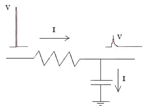
These passive low-cost solutions are very effective for VCC faults and fairly low voltage but potentially high-current failures. However, it is the high-voltage spikes that can and do wreak havoc. For example, even our 22 Ω example will still allow 363 A of instantaneous current during a typical 8 kV electrostatic discharge. Here is where parallel capacitance can also limit inrush current by shunting it away from the micro's I/O line (Figure 2).

Figure 2: Passive R/C time constants can be used to limit upper-level spikes until slower-responding suppressors can engage. Note that the energy dissipated is the same (area under the curves).
Remember, static discharges are usually very fast events. As a result, the capacitor does not have to store a lot of charge. As a matter of fact, you do not want a large capacitor. It will skew signals and degrade digital performance. It just has to slow the voltage rise rate enough to allow circuits to absorb the energy in a more controlled way. This is fine for low-speed signals in a possible EMI-filled environment like in some automotive designs.
Countless discretes and even R/C arrays can be used to tap multiple I/O lines that are potentially exposed. These can be used in conjunction with semiconductor transient voltage suppression technologies which can absorb and shunt higher levels pretty quickly; you want fast response times. Our 22 Ω example exposed to an 8 kV jolt will be dissipating an almost instantaneous 3 MW of power when shorted to ground.
For most normal environments, the static charge should not be more that 15 kV (but we have all been surprised by a higher than usual shock when conditions are just right). This is why often several I/O lines need to be protected, even if they do not couple to outside conductors. The small pin spacing can let arcs hop. Multi-channel ESD devices like the general-purpose TPD4E001 ESD Protection Arrays from Texas Instruments can help here. Parts like the TI TPD4E001DRLR provide bi-directional protection with a 30 kV range (+15 to –15 kV).
In addition to general-purpose parts, application-specific devices are also available for designs, such as the TI TPD4S014DSQR for USB charger port protection, or the supplier’s TPD7S019-15DBQR for VGA port protection.
Tyco also provides parts for this need from its TE Connectivity division. The Silicon ESD family (SESD) from TE are sized reduced from previous generations and the newest 0201 sized parts feature family members with very-low capacitance (0.6 pF), and selectable voltage response ranges. Single-, dual-, quad-, and hex-channel parts help with tight spaces.
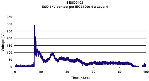
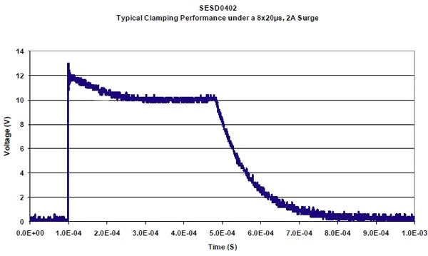
As an example, take a look at the SESD0402P1BN-0450-090. This part has a reverse voltage standoff level at 6 V. When exposed to a typical 8 kV ESD event (Figure 3), it reaches 9 V breakdown very quickly and clamps at 12 V very effectively with up to 2 A surges (Figure 4).

Figure 3: A typical 8 kV ESD event spikes rapidly, but is cut off before it reaches peak. Within nanoseconds, surges have stabilized and transient charges have discharged.

Figure 4: While withstanding an ESD event, breakdown occurs fast enough to clamp at or below rated levels.
Conclusion
When interfacing digital circuitry with the outside world, care must be taken to protect sensitive electronics. For a long time, engineers have left it up to microcontroller suppliers to provide inherent protection for I/O lines. While they do a pretty good job, increasingly, electronic equipment is more easily glitched by ESD.
Now that die sizes are the size an I/O pad used to be, we may need external protection, especially from ESD. Fortunately, several technologies provide solutions if you know where to look. For the most part, the circuitry required to provide the necessary protection is small, inexpensive, and easy to understand. Overall, MCU protection just requires a bit of forethought when designing the system to avoid numerous difficulties once the system is deployed.
For more information on the parts discussed in this article, use the links provided to access product information pages on the DigiKey website.
References
免责声明:各个作者和/或论坛参与者在本网站发表的观点、看法和意见不代表 DigiKey 的观点、看法和意见,也不代表 DigiKey 官方政策。


