Protecting Energy-Storage Devices in Energy-Harvesting Designs
投稿人:电子产品
2016-05-18
As with any electronic circuit, energy-harvesting designs can fail catastrophically when transient voltage surges exceed component ratings. With growing interest in leveraging energy harvesting in very low-voltage wearables and IoTs, designers need to remain acutely aware of the sources of destructive voltage surges and methods for their mitigation. By recognizing the need for transient voltage suppression (TVS) devices early in the design process, engineers can build robust designs better able to survive the many sources of transient voltage surges.
Transient voltage surges result from a sudden release of energy associated with power-source fluctuations, sudden load changes, coupling effects, lightning, and electrostatic discharge (ESD), among others. For circuit designers, the energy bursts underlying transients often originate in locations and due to circumstances far removed from the affected circuits. For example, a distant lightning strike's intense electric and magnetic field can couple into data and power lines, resulting in a large surge voltage well removed from the lightning strike itself.
ESD results from conditions that allow electrical charge to build up from contact and separation of two nonconductive materials until the charged body comes into contact with another object of lower potential. For example, walking across a carpet on a particularly dry day can result in a charge of 35 kV (Table 1). If applied to an unprotected wearable device or IoT system, the ESD transient would likely permanently damage sensitive digital circuits in particular.
| Means of Generation | 10-25% RH | 65-90% RH |
|---|---|---|
| Walking Across Carpet | 35,000 V | 1,500 V |
| Walking Across Vinyl Tile | 12,000 V | 250 V |
| Worker at a Bench | 6,000 V | 100 V |
| Poly Bag Picked up from Bench | 20,000 V | 1,200 V |
| Chair with Urethane Foam | 18,000 V | 1,500 V |
Table1: A simple walk across a carpet on a particularly dry day can result in an ESD transient large enough to permanently damage electronics designed with insufficient protection against transient voltage surges.
A similar problem arises when charge builds as a power or USB cable drags across a carpet or is handled by an individual who already has developed a static charge. When the individual touches the cable to a wearable's power port or an IoT device's communications port, transients from the sudden energy discharge could result in permanent damage to the electronic systems.
Internal protection
Most ICs contain internal protection circuits intended to prevent failures due to ESD strikes that might occur during manufacturing and assembly. A common approach for internal protection of I/O lines relies on a diode array designed to steer the surge current into the power supply rails, where the energy of the transient voltage pulse is dissipated. A positive surge pulse will be clamped to a voltage that is equal to a forward diode voltage drop above the supply voltage (VDD). Because the VSS pin is typically grounded, a negative pulse will be clamped to a voltage of one diode drop below ground.
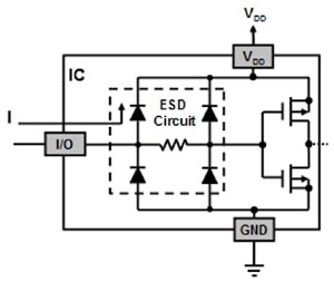
Figure 1: Semiconductor manufacturers use a variety of proprietary methods to provide device-level protection including use of internal diode arrays to steer current away from sensitive circuits within an IC. (Courtesy of ON Semiconductor)
Internal protection circuits are typically able to prevent ESD failures that occur in assembly but are often inadequate for protecting against surge events that occur in normal product usage. The semiconductor industry reflects this difference in the use of both device-level and system-level models for characterizing ESD protection. The human body model (HBM) or charge device model (CDM) are device-level specifications meant to provide protection of the isolated device during manufacturing and assembly. HBM testing is formally specified in the ANSI/ESDA/JEDEC JS-001 standard. IEC 61000−4−2 and ISO 10605 are used to represent system-level usage and reflect much higher and faster voltage-surge waveforms (Figure2).
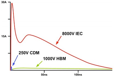
Figure 2: Device-level protection standards specify significantly lower current levels than system-level standards — representing the expected transient surges that might be found during assembly and usage, respectively. Although datasheets for diverse semiconductor devices may provide HBM ESD ratings, system-level ratings are typically included only for protection ICs or those targeting harsh environments. (Courtesy of Texas Instruments)
The lack of system-level ratings for most semiconductor devices is a matter of cost and efficiency. The surge suppression ability of a diode is directly related to its junction area, and as technology nodes continue to shrink, the integration of robust system-level ESD protection becomes significantly more costly and difficult. Consequently, internal protection remains limited not only in the level of protection but also in the number of surges. In contrast, external TVS devices are able to allocate sufficient chip real estate to provide system-level protection and to provide immunity for an indefinite amount of surges.
An external TVS device is designed to limit the current through a protected IC by decreasing the magnitude of the surge voltage. An ideal external TVS device will turn on before the IC's internal protection circuit and bleed off all of the energy of the surge. In reality, both the external and internal protection circuits will usually turn on during a surge event. As long as the current flowing through the IC's internal protection circuit remains limited to a low value, the IC's reliability will remain largely unaffected.
Among alternatives for external transient protection devices, TVS diodes typically offer lower operating voltage levels, lower capacitance, and lower dynamic resistance values compared to other transient suppression devices such as varistors and thyristors. In addition, TVS devices are able to return to their high-impedance state very quickly, resulting in a high ESD multi-strike absorption capability.
Critical layout
Even with efficient TVS devices, efficient protection depends critically on the physical layout of the design. As a general rule, the ESD device should be located as close as possible to the point of entry of expected electrostatic discharges with a power supply bypass capacitor placed as close as possible to the positive supply rail (VP) pin of the device as possible. At the same time, designers need to minimize PCB trace lengths to the power supply, ground planes, and between the signal input and the ESD device to reduce stray series inductance on the supply rail and input line to the device being protected (Figure 3).
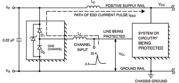
Figure 3: Efficient PCB layout is critical for reducing transient voltages, and newer TVS devices such as the ON Semiconductor CM1293A-02SO combine a pair of diodes (D1 and D2) with an integrated Zener diode to reduce parasitic series inductance L2 on the supply rail. (Courtesy of ON Semiconductor)
Even the small parasitic series inductance from the PCB traces can lead to a significant increase in clamping voltage. To help reduce this parasitic inductance, the ON Semiconductor CM1293A-02SO integrates a Zener diode across VP and VN, the negative supply rail (left side of Figure 3). This integrated Zener diode greatly reduces the effect of supply rail inductance (L2 in Figure 3) by clamping VP at the breakdown voltage of the Zener diode.
For designs such as wearables and even IoT devices where physical space is at a premium, engineers can find TVS devices available in compact packages. For example, ON Semiconductor offers its 3.3 V ESD7381MUT5G TVS in a 0.60 mm x 0.30 mm XFDFN package 0.3 mm in height and its CM1205-08CP TVS features eight TVS devices integrated into a single 1.3 mm x 0.65 mm wafer-level chip-scale package (WLCSP) only 0.4 mm in height.
Device characteristics
Engineers can find a broad range of available TVS devices but finding the parts that provide the best match with design requirements depends on a close look at a specific device's characteristics. A typical TVS device I-V curve exhibits a familiar breakdown effect but voltage levels above and below this breakdown voltage (VBR) are important in understanding TVS performance (Figure 4). Unlike Zener diodes where breakdown voltage decreases as the PN junction temperature increases, TVS devices are avalanche devices where the breakdown voltage increases as the PN junction temperature increases. Consequently, engineers might need to take temperature into account in determining specific characteristics at ambient temperatures differing significantly from the standard 25°C.
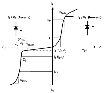
Figure 4: The IV curve for a typical unidirectional TVS device the relative voltage levels of the key specifications: working peak reverse voltage (VRWM), breakdown voltage (VBR), and clamping voltage (VC). An ideal bidirectional TVS device will show the same forward and reverse characteristics. (Courtesy of Toshiba)
At the lowest threshold, the reverse working voltage VRWM (also called stand-off voltage, Vst-off), the device appears off and only its parasitics and leakage current affect the circuit. VRWM is typically 10 to 15 percent lower than the reverse breakdown voltage VBR (also called the Zener voltage, VZ, for Zener-based devices), where the TVS device begins to conduct, entering its avalanche region. Finally, the clamping voltage, VC, is typically 35 to 40 percent higher than VBR and represents the maximum clamping voltage of the device at a specified peak impulse current IP.
Peak power dissipation (PPP) is of course a very important characteristic. Manufacturers measure PPP by forcing a specified current waveform through the TVS at increasing levels while monitoring device voltage and current. The most common waveforms used in peak-power measurements are 8/20 μs and 10/1000 μs current waveforms. (In this notation, the first value describes the waveform's rise time in μs and the second value describes the time in μs at which the waveform falls to half of its peak value.) Although PPP is not always explicitly listed in device datasheets, engineers can derive it simply by multiplying peak pulse current (IPP) by clamp voltage (VC):
PPP = VC x IPP
Dynamic resistance (RDYN) is another important characteristic for determining the suitability of particular protection IC. As current flows through the protection device during a transient surge, RDYN will result in a further voltage drop.
For a particular application, the most suitable TVS device is one with VRWM equal to the maximum continuous-DC or peak-AC voltage the application circuit will experience in normal operation. At the same time, engineers need to ensure that VC does not exceed the instantaneous voltage level acceptable for safe operating conditions of the other components in the circuit. Finally, RDYN must be sufficiently low to ensure that at peak current the device's own dynamic resistance does not cause the clamping voltage to rise beyond acceptable limits (Figure 5).
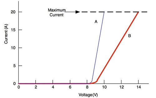
Figure 5: Even if two devices A and B specify the same breakdown voltage and peak current, if device B has higher dynamic resistance (RDYN) than device A, device B might be a less effective protection device because it reaches a higher clamping voltage (red line). (Courtesy of ON Semiconductor)
Finally, engineers can take advantage of combinations of devices with different working voltages to provide additional protection in high-voltage applications such as solar-energy harvesting. For this type of application, designers can use multiple TVS devices with different VRWM specifications to reduce the total energy a single TVS device might have to dissipate in a high-voltage transient event (Figure 6). Here, a device such as the Vishay SMBJ24D (24 V VRWM) would provide primary protection. A following series resistor would reduce current reaching a device such as the Vishay SMBJ5.0CD (5 V VRWM). To further reduce the impact on the protected IC's internal protection circuitry, engineers could place another series resistor between the second TVS device and the IC.
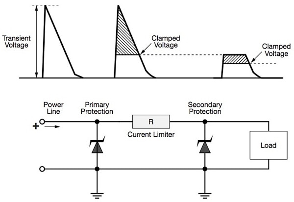
Figure 6: Engineers can mitigate effects of very large transient voltage surges by using additional TVS devices where the primary device delivers a reduced surge to the secondary device for further suppression. An interposing series resistor reduces current reaching the secondary device and ultimately, the load. (Courtesy of Vishay)
Conclusion
As the industry moves increasingly toward lower-voltage designs, circuits without protection from transient voltage surges face the threat of degraded performance and even permanent damage. Available with a broad range of performance characteristics, TVS devices offer a cost-effective solution for protecting these sensitive designs. By including TVS devices early in the design stage, engineers can deliver robust designs more capable of withstanding the effects of transient voltage surges.
For more information about the parts discussed in this article, use the links provided to access product pages on the Digi-Key website.
免责声明:各个作者和/或论坛参与者在本网站发表的观点、看法和意见不代表 DigiKey 的观点、看法和意见,也不代表 DigiKey 官方政策。


