Package-Related Thermal Resistence of LEDs
投稿人:Convergence Promotions LLC
2010-12-22
In order to achieve the expected reliability and optimal performance for today’s standard light emitting diodes (LEDs), the use of appropriate thermal management is advantageous in most cases. For modern high power LEDs with a power dissipation of several Watts, this is essential.
Basically, the operation of LEDs is limited by various factors, depending on the material and technology deployed. An important parameter of practical interest for users is the temperature of the active semiconductor layer (junction temperature), since this influences the function and lifetime of the LED. The manufacturer’s recommended maximum junction temperature should therefore not be exceeded during operation in order to prevent damage to the component. The goal in the development of thermal management is to keep the junction temperature as low as required for the given application. An important aid in the development of thermal management is the thermal resistance (Rth) of the LED.
Ideally, the user requires a thermal resistance that describes the thermal characteristics of the component independent of the environmental conditions and allows the user to determine the junction temperature of the LED with sufficient precision.
In practice, however, an environment-related thermal resistance Rth,JA is specified, which is determined under defined measurement conditions (see JEDEC 51). Under real technical conditions of use in an electronic device, however, deviations from these conditions arise. Those influence the accuracy of determining the junction temperature.
An exact determination of the junction temperature is therefore only possible if self-determined, device-related correction factors are available to the user. For the majority of users, however, this is probably not the case.
Thermal resistance Rth
The thermal resistance (Rth) or absolute thermal resistance is defined as the rate of temperature increase for the supplied power and, in the end, is a measure of the capability to dissipate heat.

The temperature increase of LEDs is caused by that portion of the power dissipation that is not transformed into light. The temperature difference ΔT, or upper temperature is therefore defined as the difference of the inner temperature of the heat source (semiconductor chip) and an external constant reference temperature. Since the temperature increase is proportional to the power dissipation, the thermal resistance Rth can also be seen as the proportionality factor that contains the physical heat dissipation characteristics of the LED in question.
Knowledge of the thermal resistance Rth of an LED serves to:
- determine the junction temperature that arises in the LED under operating conditions
- determine the maximum allowable external reference temperature for a given internal temperature and power dissipation
- evaluate measures for dissipation of heat (thermal management)
For the definition of the thermal resistance Rth of an LED, two temperatures are required — the inner temperature of the heat source and an external reference temperature (temperature of an external point on the component).
For an LED, the “temperature of the inner heat source” refers to the temperature of the active semiconductor zone in which the photons are generated. This is designated as the junction temperature TJ.
The appropriate selection of the external temperature reference point depends on the type of housing and the respective rate of heat dissipation.
For an OSRAM Opto Semiconductors SMT LED (such as the TOPLED® or DRAGON® LED, for example) this reference point is the “solder point” TS or for an LED (such as the OSTAR®-Lighting), the “board” temperature TB.
Here, the “solder point” is the transition from the active heat path of the housing to the solder surfaces of the circuit board and is dependent on the packaging technology. For components like OSTAR®, the “board” temperature refers to the underside of the components.
TOPLED® product family
The primary flow of heat for TOPLED® packages occurs by the transfer of heat from the chip and leadframe to the ends of the thermally active leads. It should be noted here that depending on the design of the semiconductor housing, a differentiation can be made between thermally active and inactive leads. Thermally inactive leads are those which are only connected to the chip by bond wires.
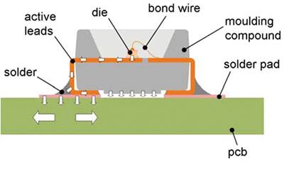
For these components, the solder point temperature can be directly determined in practice by gluing a thermo element at or on the solder pads of the thermally active leads/pins (see also application note Temperature Measurement with Thermocouples).
DRAGON® LED product family
In the case of the DRAGON® product family, the internal dissipation of heat from the chip occurs primarily via the integrated heat sink to its underside.
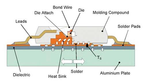
Here, the practical measurement of the solder point temperature is a bit more complicated since the temperature cannot be directly measured at the heat sink. Instead, it is recommended to record the temperature directly adjacent to the DRAGON® housing on the long side by means of a thermo element on the circuit board. Steady state the temperature gradient to the heat sink is negligible in this case.
OSTAR® product family
For the OSTAR® product family, the internal dissipation of heat occurs from the chip via the ceramic sub-mount to the underside of the carrier board (Figure 3).
Definition of power loss and heat flow
With classical silicon-based semiconductor components such as integrated circuits and transistors, the entire electrical energy is converted into heat. The heat flow can therefore be equated to the electrical power loss and leads to a clear interpretation of the thermal resistance.
With light emitting diodes (LEDs) however, the supplied electrical energy is only partially converted to heat. Depending on the optical efficiency, a portion of the electrical energy is emitted as light/radiation (optical energy).

This leads to two different definitions of thermal resistance for LEDs.
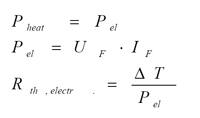
Electrical thermal resistance
The thermal resistance is defined in the same manner as classic semiconductor components. The energy coupled out (light/radiation) is not taken into consideration (see JEDEC 51).
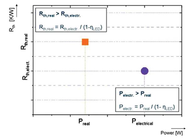
Real thermal resistance
This definition of thermal resistance considers the actual flow of heat that is dissipated through the housing. The optical power of the LED that is coupled out is therefore taken into consideration.
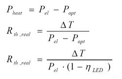
where: ηLED = optical efficiency of the LED
This value is independent of the working point of the LED and can therefore be used to characterize the LED housing. Through the use of the real thermal resistance when considering the thermal layout, it can be guaranteed that the maximum permissible junction temperature is not exceeded for all modes of operation that arise.
Consequence of the two thermal resistances
For a better understanding of the two different thermal resistances, the issue, and their effect will once again be addressed and clarified by means of a comparative example.
Normally, for the development of an application and especially in the evaluation of appropriate thermal management, one starts with a predefined thermal resistance and the expected increase in temperature ΔT (= Tj,max –Tambient), that determines the maximum permissible power or current.

Depending on which thermal resistance is drawn upon for the calculation (Rth,electr or Rth,real), different maximum permissible powers or currents result.
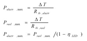
It should generally be noted here, that in principle, these powers or currents only describe the initial state (= 0h) for maximum LED efficiency and minimum power consumption. For the calculation that uses the thermal resistance Rth,electr., this means that at the beginning (t = 0h), the maximum junction temperature Tj,max has been reached.

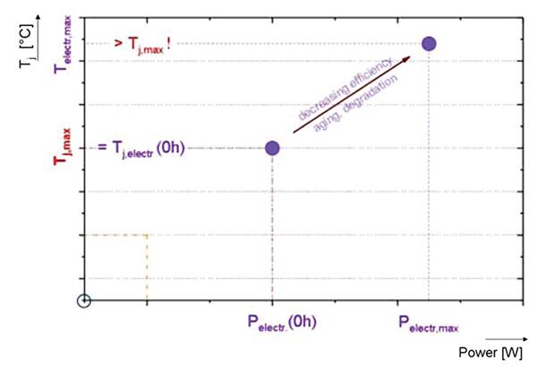
Progressive aging and sustained temperatures lead to a decrease in optical efficiency, however, and therefore to an increase in power consumption. This in turn leads to an increase in the junction temperature. For the calculation that uses the thermal resistance Rth,electr., this means that:

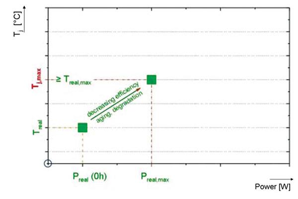
The same increase in junction temperature also applies for the calculation of the maximum power with the real thermal resistance Rth,real.
In this case, however, since the optical efficiency is also taken into consideration, the maximum achievable temperature is limited by the maximum permissible junction temperature.

Determination of the thermal resistance Rth,JS at OSRAM OS
OSRAM Opto Semiconductors uses the thermal transient measurement method, which is called the static thermal resistance test method according to JEDEC 51, in order to determine the thermal resistance of OSRAM Opto Semiconductors LEDs.
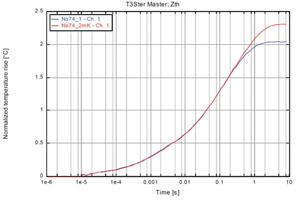
The temperature is measured with a temperature-sensitive parameter of the LED - the forward voltage drop of the diode. However, the accurate and reproducible measurement of junction to solder point thermal resistance Rth,JS is far from trivial and up to now, not defined by international standards.
In order to determine the thermal resistance Rth,JS, the device under test has to be measured twice. For the first transient thermal measurement, the device is applied to the heat sink (isothermal plate) without thermal grease; the second measurement is done with the same setup but with thermal grease. For low power LEDs, different PCB materials are used.
Figure 7 shows two Zth-curves of an OSTAR® module which has been measured with and without thermal grease between board and the water-cooled cold plate. The transient thermal behavior of the device in this two-measurement setup is identical as long as the heat propagates from the junction through the device. When arriving at the solder point or the end of the board to heat sink interface, the curves are different depending whether or not thermal grease is present at the interface. This change in the ambient condition indicates the end of the device. Therefore the Rth,JS value can be determined as the value Zth(ts) at the point of time “ts” when the two curves start to separate.
Thermal resistance Rth,JS in the LED datasheets from OSRAM Opto Semiconductors
In the data sheets from OSRAM Opto Semiconductors, the value Rth,JS is specified by:

The data refers to the real thermal resistance.
For comparison the effective thermal resistance (Rth,electr. = Rth,effective) is also listed by the high power LED devices.
These are determined by means of measurements of a random characterization test and entered into the data sheets in the following manner:
Standard LED
(e.g. TOPLED, PowerTOPLED)
In the data sheets for these components, the maximum value of the thermal effective resistance is specified.

The maximum thermal resistance is statically determined from the distribution of the random characterization test.

IR devices
In the data sheets for the IR components, the data sheet contains the typical thermal resistance of the sample characterization test and the resulting maximum thermal resistance.

High power LEDs
(e.g. Advanced PowerTOPLED, DRAGON LED, OSTAR)
In the case of the high-power LED, the data sheet contains the typical thermal resistance of the sample characterization test, the resulting maximum thermal resistance, and for comparison the effective thermal resistance with the optical efficiency of the LED.
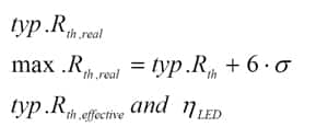
By stating the typical thermal resistance, the comparability of different housing packages is guaranteed.

免责声明:各个作者和/或论坛参与者在本网站发表的观点、看法和意见不代表 DigiKey 的观点、看法和意见,也不代表 DigiKey 官方政策。


 中国
中国