New Automotive Power Module (APM) Inverter Reference Design
2015-08-25
Introduction
Fairchild Semiconductor has developed an inverter reference design (IRD) demonstrating the use of the new FTCO3V455A1 three-phase automotive power module (APM). It is intended for use in medium power (1-2 kW) 12 V three-phase inverter applications. It is most suitable for automotive applications such as electric power steering, electric air conditioning, transmission lube-pump and other vehicular applications. The IRD kit is intended to provide a quick and inexpensive platform for the evaluation and application of the APM in a complete three-phase inverter configuration. Simply add the appropriate electronic system controls and a motor drive solution can be realized with minimal time and investment. The photograph of the IRD is seen in Figure 1.
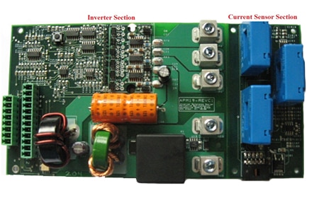
Figure 1: IRD photograph.
Features
- FTCO3V455A1 Three-Phase Power Module
- Optical Input Isolation
- Three Half-Bridge Gate Drivers
- Inverter DC Link Current Shunt Amplifier
- Module Temperature Conversion Circuitry
- Sensed Phase Voltage Amplification for Feedback
- Overcurrent and Over-Temperature Shutdown Circuitry
- Reverse Battery and Voltage Transient Protection Circuitry
- Optional Three-Channel Current Sensor Board (typ. 2-Phase plus DC Link)
System Overview
The Inverter Reference Design (IRD) evaluation board, with optional three channel current sensor board, demonstrates the usage of the automotive power module. This article contains a complete description of the power module, inverter drive, signal conditioning and the typical operating characteristics. The system block diagram is shown in Figure 2.
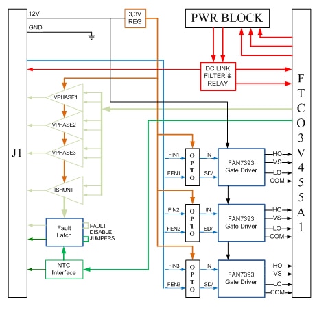
Figure 2: IRD block diagram.
The control power for the entire IRD is derived from a single 12 V input source. In addition, the system must be supplied with a high-current battery source, used to power the load motor via the inverter bridge. A single 12 V supply can be used to provide power for both of these functions, if desired.
The high-current battery source is connected through a DC link relay and a differential/common-mode filter network before its application to the inverter-bridge. The relay control circuitry provides a reverse battery protection scheme where the relay will not energize unless the battery source is connected with the proper polarity and with a sufficient voltage level.
The DC link filtering is provided to reject common-mode battery voltage source noise by use of a Y-capacitor and a common-mode choke. The inverter-bridge voltage is further filtered by an L-C PI network and a pair of differential-mode capacitors.
A 3.3 V linear voltage regulator circuit is derived from the 12 V control source and used to power all of the logic and amplifier circuitry.
Since the gate-drive circuitry needs to maintain a sufficiently high output voltage to assure full gate drive to the APM, the three gate driver devices are powered directly from the 12 V control source.
The switching of the inverter-bridge devices is controlled by eight digital input signals (6 gates, relay control, and fault clear), which are connected through an array of opto-couplers. These inputs are referenced to a single common digital input connection and are completely isolated from all other IRD circuitry. This floating common connection can be connected to the board ground or remain completely isolated to provide superior controller noise immunity.
The analog output and digital output signals are referenced to the board common ground (GND). The range, scaling and descriptions of these I/O signals are detailed in Table 1.
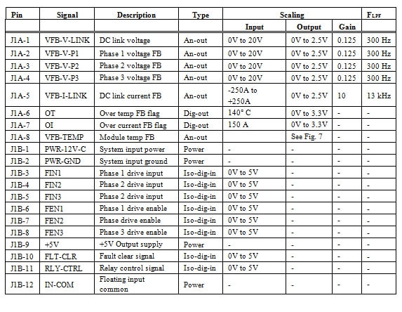
Table 1: Signal I/O connections.
Module description
The APM contains a three-phase MOSFET bridge, current sense shunt, R-C voltage snubber circuitry and a temperature sensing thermistor (NTC). It has fourteen signal connections on one edge and five power connections on the other. These nineteen connections are soldered to pads on the IRD. The module also has an electrically-isolated copper heat spreader on the bottom side, which must to be connected to an external heatsink. The schematic of the module is shown in Figure 3.
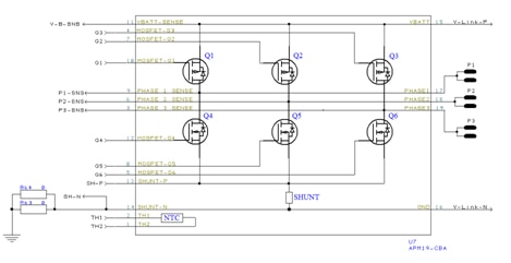
Figure 3: Power module internal schematic.
Input Isolation
The isolation of the inverter drive and input control signals is accomplished by the use of dual high-speed input signal opto-couplers. Each of the eight digital input channels is optically isolated using a photocoupler and has a common ground connection to the IN-COM pin.
This circuit configuration provides complete isolation between the inverter and an external microcontroller. Since the opto-coupler inputs are current driven, it will operate over a wide range of input voltage. The input voltage must provide at least 2 mA of photo diode drive current and not more than 20 mA. Therefore, the minimum “logic-high” input level signal is any voltage above 5 volts, and can be as high as 20 volts. A “logic-low” level signal is any voltage lower than 1.6 volts. Lower input voltage levels can be accommodated by reducing the value of the opto-coupler input resistors.
Gate Driver
Mounted on the IRD is the three-phase power module, containing six individual MOSFET devices. Each of the MOSFET devices requires a gate drive current amplifier for their control. These current drive functions are provided by three half-bridge gate driver ICs.
The gate driver stage consists of three FAN7393A half-bridge gate driver ICs, one for each leg of the power bridge. Each of the gate driver ICs requires three input signals: not_shutdown (SD/), input (IN) and dead-time (DT).
The dead-time signal is used to adjust the dwell time applied between the turn-off of one device and the turn-on of another (in a given phase leg) to avoid a short circuit or “shoot-through” condition. This time is set by means of a single programming resistor, connected from the DT terminal to ground. Initially, the programming resistor’s value is set to 22 kΩ, which will provide a 1 µs lock-out period.
The resistor network on the output of the gate drive IC provides bi-directional gate driver output currents. This configuration will provide one-half of the gate resistance during device turn-off, versus that used during device turn-on. This permits the power device turn-on and turn-off times to be adjusted independently.
Amplifiers
On-board amplifier circuits are provided to condition the three-phase voltages, the DC link voltage, current shunt signal and the NTC thermistor. The three-phase voltages and DC link voltage are monitored via a group of operational amplifiers, arranged in a modified differential amplifier configuration. A voltage dividing input filter network is used to limit the absolute voltage applied to the amplifier’s ICs and provide a low-pass filter.
An example of one of the low pass filter circuits is shown in Figure 4. The cutoff frequency, signal range, gain and offset parameters are detailed in Table 1.
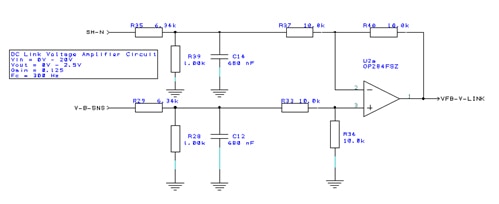
Figure 4: Voltage amplifier circuit.
The voltage amplifiers are designed such that the high-frequency switching components of the signal will be eliminated, leaving only the motor fundamental frequency. These filtered voltage signals are available on the output connector (refer to Table 1). The module’s internal current shunt signal is also amplified in a similar manner.
The current shunt amplifier’s DC gain and filter cutoff frequency are shown in Table 1. This amplifier is capable of processing the shunt’s low-level signal into a useful high-level control signal. The converted current signal is available on the output connector. It is also connected to the overcurrent detection circuit, where its signal level is compared to a voltage reference which is set to a level indicative of an excessive current condition. Any shunt current level in excess of 150 A will trip the overcurrent fault circuit which will disable the inverter-bridge, assuming the overcurrent fault enable jumper is in place. The overcurrent fault signal will appear at the I/O connector, regardless of the state of the jumper and can therefore be used in the control software independent of the on-board overcurrent fault detection circuitry.
The APM module contains an internal thermistor, which is mounted close to the MOSFET die in order to provide over-temperature protection of the module’s power devices.
The module’s temperature signal level is compared to a voltage reference indicating an over-temperature fault (OT) condition. Any voltage level indicating a temperature in excess of 140°C will trip the over-temperature fault circuit, assuming the over-temperature fault enable jumper is in place. The over-temperature fault signal will appear at the I/O connector, regardless of the state of the jumper and can therefore be used in the control software independent of the on-board over-temperature fault detection. The over-temperature and over-current trip levels can be changed by adjusting the resistor values that set the comparator reference voltage levels.
Fault Protection
The IRD has on-board fault protection circuitry which can protect the power module in the event of a serious overcurrent or over-temperature condition. When jumpers J2 and J3 are in place, the overcurrent (OI) and over-temperature (OT) signals are connected to the fault protection circuitry. During a fault condition, the protection circuit will override the three input enable signals which will disable all three gate driver circuits. Once a fault is triggered, the fault LED will glow red, indicating that a fault has occurred and that the inverter has been latched into an idle state.
Once a fault has occurred, the inverter can be reset in any of three different ways:
- Cycle the control power supply off and bring it back on again
- Press the reset push button on the PCB
- Present a logic “high” signal at the FLT-CLR terminal with respect to the IN-COM terminal on the I/O connector.
The fault protection circuit is shown in Figure 5.
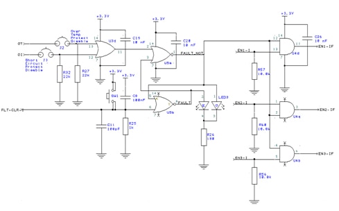
Figure 5: Fault protection circuit.
DC Link Filter and Relay
The high-current battery source is connected to the IRD via the “power block” POS and NEG terminal connections. It is connected to the inverter-bridge through relay K1 and is then filtered by a common/differential mode and pi filter networks. In addition, transient voltage protection is provided by TVS and Zener clamp devices. The relay is controlled by a low-side MOSFET switch, which is operated by an external isolated digital input signal. Reverse battery protection is implemented by the fact that the relay can only be energized if the battery voltage is present and correctly polarized. The DC link filter and relay circuitry is shown in Figure 6.
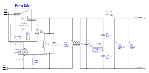
Figure 6: High current battery source filtering circuits.
Current Sensor Board
The IRD system offers an optional three-channel current sensor board that mounts directly in the output area of the IRD PCB. Each of the three current sensor channels include a band limited low pass filter (LPF) circuit, used to control the current sensor system output bandwidth. The three channels can be used for the measurement of the three phase currents. Or they can be used for measurement of the DC link current and two phase currents.
The three current sensors used are the LEM HAIS-100P and are rated at 300 amp peak current. The sensors have a 5 V output range, with a 2.5 V offset corresponding to the zero current input signal.
This article first appeared on the Fairchild Blog.
免责声明:各个作者和/或论坛参与者在本网站发表的观点、看法和意见不代表 DigiKey 的观点、看法和意见,也不代表 DigiKey 官方政策。


