Microinverters Improve Efficiency
投稿人:电子产品
2011-06-30
Microinverters designed to convert the DC power from a single solar panel to the AC supply required by the grid, are grabbing significant market share from conventional string or central inverters.
While still in its infancy, the microinverter market is growing apace, particularly for small rooftop applications that suffer from partial shading. UK-based analyst IMS Research predicts that microinverters will serve more than 1 GW of global photovoltaic installations by 2013, which will equate to around five percent of the total installed capacity.
The popularity of these modules is not surprising, considering their advantages over traditional inverters. These advantages include ease-of-installation, localized maximum power point tracking (MPPT) and robustness due to built in redundancy.
Because it’s still early in the microinverter development cycle there are a number of topologies vying for dominance. These topologies can be broken down into two broad categories: single-stage and two-stage. Let’s compare these two types and illustrate their implementation with circuit schematics based on National Semiconductor’s SolarMagic ICs.
Coping with shade
Installation of solar panels onto domestic rooftops has been encouraged via tax credits or other financial incentives by several national governments. The U.S., Australia, Germany, and Spain are examples of countries that have introduced such schemes.
A common downside of such domestic installations is that, because the rooftop position is fixed and isn’t necessarily perfectly aligned with the sun’s arc across the sky, some panels can be shaded during the day, reducing overall output.

Figure 1: Rooftop solar panels can suffer from partial shading, reducing overall output.
The string converters commonly used for photovoltaic panel DC-to-AC conversion compound the problem. This is because a single inverter is connected to a series of panels and its output is restricted by the performance of the lowest output panel. In other words, a single shaded (or partially shaded) panel will lower the output of the entire group to its voltage output level. Studies have shown that shading of as little as nine percent of the panel array can reduce its output by up to 54 percent.
Microinverters have gained in popularity because they overcome this problem by feeding each single panel’s output to a dedicated inverter. Consequently, a shaded panel’s output can’t drag down the voltage of other panels in the group. Manufacturers claim that an installation’s efficiency can be raised by at least five percent, and up to as much as 20 percent, by exchanging a string inverter for one microinverter per panel.
Single-stage microinverter
Figure 2 shows a schematic of a microinverter using a single-stage topology[1]. The DC-to-DC converter outputs a rectified sinusoidal waveform that’s then inverted into a full sinusoidal waveform – suitable for the grid – by an “unfolding bridge”.
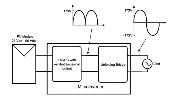
Figure 2: Schematic of microinverter using a single-stage topology. (Source: National Semiconductor)
Although it would appear that this is actually a two-stage device, it is categorized as single-stage because panel voltage boosting and shaping of the AC waveform is achieved in a single stage.
The most widely adopted circuit for a single-stage microinverter is a quasi-resonant interleaved flyback (other circuits include – non quasi-resonant – interleaved flyback and interleaved forward converter). The unfolding bridge inverter is generally implemented using four silicon controlled rectifiers (SCR) switching at the grid frequency.
Figure 3 shows a simplified schematic of a quasi-resonant interleaved flyback based on National Semiconductor’s SM72295 Photovoltaic Full Bridge Driver. Using the SM72295 in this circuit maximizes power density, reduces component count, and decreases PCB area.
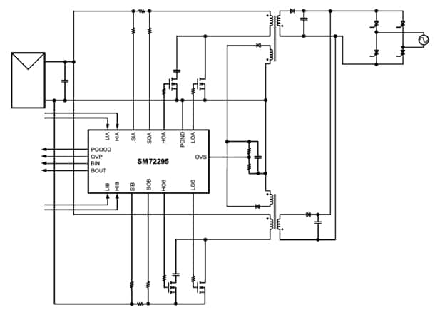
Figure 3: Simplified schematic of a quasi-resonant interleaved flyback using the SM72295. (Source: National Semiconductor)
The SM72295 combines four independent metal oxide semiconductor field effect transistor (MOSFET) gate drives with signal conditioning, power good, and overvoltage sensing functionality. Gate drive signal inputs are compatible with 3.3- and 5-V logic.
Single-stage microinverters have a number of advantages, including lower component count, low switching frequencies for the unfolding bridge, and the ease with which isolation can be implemented. There are some drawbacks though. These include high voltage ratings on the primary side switches and secondary side diode, and a high amplitude 120-Hz ripple current at the input.
This input ripple current must be reduced – by large electrolytic capacitors – to minimize power losses. The introduction of these electrolytic capacitors into the circuit, however, can compromise long-term reliability.
Two-stage microinverter
The second popular category of microinverter, the so-called two-stage type, employs a DC-to-DC converter with high voltage output, an intermediate high voltage DC bus, and then a conventional pulse width modulated (PWM) controlled MOSFET or insulated-gate bipolar transistor (IGBT) full bridge to modify the output for grid suitability. The DC-to-DC converter features a high boost ratio to raise the output from the photovoltaic panel to the intermediate bus voltage. Figure 4 illustrates a schematic of a two-stage microinverter.
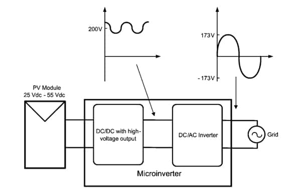
Figure 4: Schematic of two-stage inverter with intermediate high voltage DC bus. (Source: National Semiconductor)
They are several popular circuits for the DC-to-DC conversion stage, including interleaved flyback, push-pull converter (current feed or voltage fed), and full-bridge converter (current fed, voltage fed, or resonant).
Figure 5 shows a simplified schematic of a two-stage microinverter using a voltage-fed full bridge for the DC-to-DC converter and a MOSFET full bridge for the DC-to-AC inverter stage. Again, the implementation is based on the SM72295 that provides gate drives for the four primary side MOSFETs.
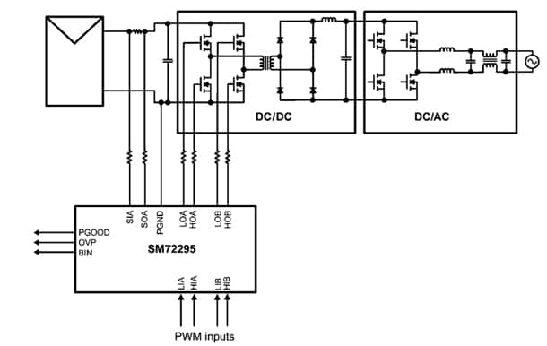
Figure 5: Simplified schematic of a two-stage microinverter. The DC-to-DC stage is implemented as a voltage-fed full-bridge converter, and the DC-to-AC stage is realized as a MOSFET full bridge. (Source: National Semiconductor)
The device is capable of driving all four MOSFETs in the primary-side full bridge. The chip provides two high-side and two low-side gate drives, integrated bootstrap diodes, and is suitable for input voltages up to 100 V.
Because they use additional high frequency switching components, two-stage microinverters are more expensive than the single-stage type. However, because consumers expect microinverter mean time between failures (MTBF) of at least a decade, reliability can be more important than cost. The use of a two-stage topology lowers the photovoltaic input ripple current, allowing the design engineer to employ high reliability film capacitors instead of the less robust electrolytics typical of single-stage designs.
Two-stage microinverters are able to supply reactive power (whereby voltage and current are 90 degrees out of phase) to the grid, which is not possible with a single-stage module using an SCR unfolding bridge. This is an increasingly significant advantage as a growing group of countries mandate a requirement for reactive power output from larger photovoltaic installations.
免责声明:各个作者和/或论坛参与者在本网站发表的观点、看法和意见不代表 DigiKey 的观点、看法和意见,也不代表 DigiKey 官方政策。


 中国
中国