Microcontrollers for Sensors and Data Acquisition
投稿人:Convergence Promotions LLC
2013-05-01
Early microprocessors and microcontrollers were pure digital devices having nothing to do with analog functionality. However, the advantage of having on-chip A/Ds and D/As became quickly apparent and today you would be hard pressed to find a microcontroller family that does not have some form of mixed-signal functionality.
In fact, there is a flurry of activity supporting mixed-signal processing and system-on-chip solutions. The resolution of converters has migrated from 8 to 24 bits in some cases, and on-chip op-amps and comparators are now flexibly routed to and from converter stages. Even DSP functionality and floating point math functions are allowing firmware to be more streamlines as pipelined architectures fill with data.
This article examines a range of mixed-signal chip microcontrollers of varying sizes and features that are readily available today to support new mixed-signal designs aimed at sensor interfacing. All parts, datasheets, and referenced materials can be found on DigiKey’s website.
Size matters
Remote and distributed sensor systems call for a small, low-power processor that will either run on batteries, energy harvesting, or remote power supplied through long runs of cable. In any event, remote sensors need to be small, rugged, reliable, and able to operate on a very limited power budget.
A case in point is the SOT 6-pin Microchip PIC10F220T-I/OT, which contains two 8-bit A/D converters (see Figure 1). An internal 8 MHz clock processes the 33 single-cycle instructions in 500 ns using a two stage pipeline; the micro goes into standby mode draining only 100 nA at two volts. Power supply range is two to five volts.
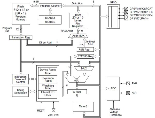
Figure 1: Housed in only 6-pins, this microcontroller has mixed-signal support targeting dedicated remote sensor applications with its limited resources and power (Courtesy of Microchip).
Note that processors in this class are mostly dedicated to very specific functions. No deep banks of RAM are on-chip and powered up. There is only 16 bytes of RAM on the PIC10F220. On-chip instruction Flash is only 384 bytes, which results in 256 instructions since instruction size is 12 bits wide (even though data paths are 8 bits wide).
It is not complicated to wake up, take a sensor reading, check thresholds or alarm conditions, and communicate before snoozing again. These parts have power-on reset, brownout detectors, and watchdog timers. Some PIC10F family members can have up to 64 bytes of RAM and a third A/D converter.
Prototyping adapters like Microchip’s AC163020 help simplify prototyping. Microchip has a family of MPLAB development systems that can help you evaluate and develop with their processors.
For more complex tasks, you will want a beefier processor that will carry with it a larger sized package. You may be surprised to know that several legacy cores have had “engine rebuilds” to keep them competitive even today.
Legacy alive
Early attempts to add analog functionality to digital microcontroller cores were awkward and carried with them notable constraints and limitations. For example, in order to use the on-chip A/D, you had to put the micro core to sleep; otherwise, you would burn a few LSB-bits of resolution with processor noise artifacts. Modern flavors of old cores solved these issues and can keep legacy code functioning.
Several manufacturers still make their own and/or other companies’ cores with some modern updates such as mixed-signal support. For example, Zilog’s Z86E8316SEG microcontroller is based on the 8-bit Zilog Z8® cores. The popular core of yesteryear still comes with 4 K OTP program space and 237 bytes of RAM, but it now it has eight 8-bit A/D converters in its smaller 20-pin flavor. While having more code space, I/O, and RAM than the smaller PIC10F220, it is still aimed at small, low cost, and low-complexity designs.
A little meatier is the 8051 core which is still alive and well with a half dozen manufacturers – such as Atmel’s AT89LP3240 – providing modern day mixed-signal versions of this old, but widely used architecture with clock speeds from 8 to 100 MHz.
If you are going to run old legacy code, you will not be taking advantage of new features, but there will be times when the performance increase that comes from single cycle instruction execution (instead of 12 cycles) will come in handy. Other 8051 limitations have been addressed by adding larger stacks and memory depths and a second index pointer.
Let’s look at the middle of the road chip - the 25 MHz Silicon Labs C8051F986-GU with 8 K of Flash and 512 bytes of RAM. While containing more RAM than older versions, the 1.8 to 3.6 V part also incorporates a ten-channel 12-bit A/D converter, as well as newer, established common communications peripherals like SPI, I²C, and UARTs. The chip is usable for low-power designs with its 10 nA sleep current (with data retention) and 150 μA/MHz active current (up to 25 MHz from 1.8 to 3.6 volts). Just for good measure, it also has an internal VREF and temperature sensor.
However, take this to the extreme with the 100 MHz Silicon Labs C8051F360-GQ that contains 17 10-bit A/D converters (see Figure 2). It also features system programmable 32 Kbytes of Flash and over 1 Kbytes of SRAM along with internal oscillators and hardware-based SPI.
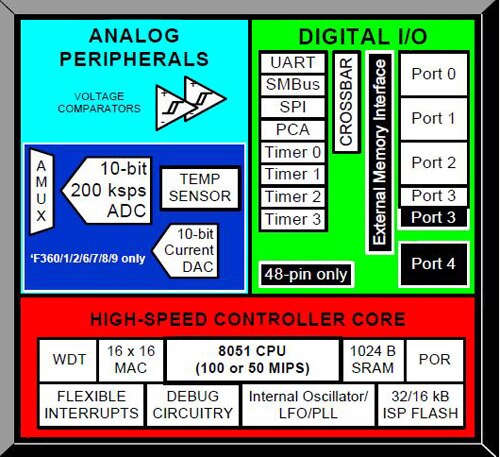
Silicon Labs has a comprehensive C8051 development kit and a ToolStick programming adapter, as well as a training module discussing its C8051 low power MCUs.
Other suppliers of 8051-based cores for mixed-signal designs includes NXP Semiconductors, Cypress Semiconductor, Zilog, and Atmel. It is interesting to note that some very high-end 8051-based cores can compete head-on with more modern cores and offer some unique flavors.
For example, the Analog Devices 8051-based ADUC847BSZ62-5 features two independent 24-bit Sigma Delta A/D converters (see Figure 3). Designed for three to five volt operation, the 52- and 56-lead packages preserve the functionality of the 8051 while adding the A/Ds, SPI, I²C, and 12-bit D/A. It adds some nice features such as dedicated high baud rate generators (eliminating the need to burn up a counter/timer) and an extended stack pointer.
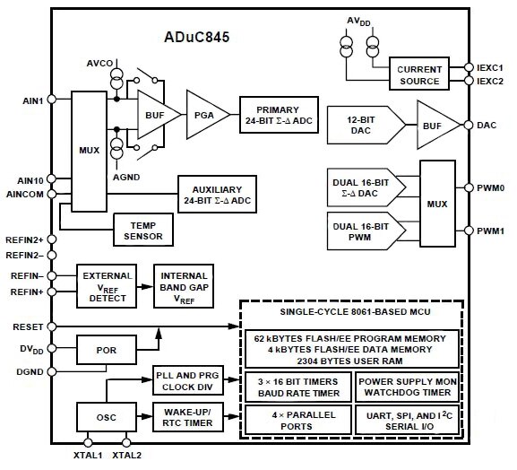
Figure 3: At the core may be an 8-bit 8051, but these parts have two independent 24-bit Sigma Delta A/D converters letting these processors handle resolute tasks that not even many 32-bit processors can in a single chip solution (Courtesy of Analog Devices).
Upping the ante: 16-bit cores do more
The 16-bit processors have enough horsepower to do a good deal of signal processing, but do not waste power keeping 32-bit data paths and memory arrays powered up. Even for non-low-power designs, a 16-bit processor may be ideal, especially when linear resolutions are limited to 16 bits.
There is often a trade-off between software complexity and development time versus efficient use of code space. When software can fill up and draw from successive memory locations without having to shift and mask non-boundary aligned data points, it makes coding, debugging, and testing easier and faster. For example, any 8-bit processor with 10- or 12-bit A/D resolution can burn up two successive 8-bit memory locations in order to store a 10-bit value. It is more memory efficient to bit-pack samples so as not to waste precious memory. However, this can impose boundary addressing constraints when writing code and using memory efficiently. A 16-bit A/D, on the other hand, that can map into a 16-bit memory location removes these constraints and inefficiencies and lets analog data live happily in its digital host.
Several 16-bit microcontrollers are readily available with a good mix of peripherals, mixed-signal elements, and raw processing power. An example is the Maxim Integrated DS4830T+ optical control microcontroller, which houses an internal 16-bit architecture with 18 10-bit A/D inputs. While designed to support optical transceiver designs for short- and long-reach 40 and 100 Gbps links, the A/Ds, DACs and PWMs can be applied to any signal processing applications that can take advantages of this 16-bit low-power microcontroller that is designed to run C code in a streamlined manner.
Another contender is Freescale Semiconductors’ MC56F8006VLC 16-bit core with up to two 28-channel 12-bit A/Ds and DSP functionality. Helping incorporate more of the analog functionality, these parts include three on-chip comparators and take aim at industrial control, home appliances, smart sensors, and security applications to name a few. The MC56F8006 is supported by Freescale’s MC56F8006DEMO demo and development kit for general-purpose application development. The kit includes a full schematic and bill of materials.
Popularity contests
One of the most widely used 16-bit processors for data acquisition and low-power designs is the MSP430 family from Texas Instruments. This is a family of processors with a common architectural structure and a variety of I/O, packages, peripherals, speeds, memory depths, and features supported by a lot of training materials, application notes, and development systems.
On the low end of the family is the small 8-pin MSP430G2230IDR, which can compete head-on with the 6-pin Microchip part discussed earlier but with an internal 16-bit wide architecture (see Figure 4). This part uses a RISC architecture to achieve 62.5 ns instruction cycle times; it also has a very fast 1 µs wakeup time. Both factors are important to reduce overall energy usage.
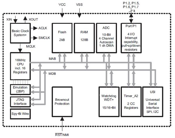
Figure 4: Four 10-channel A/D converters are available inside this 8-pin mixed-signal microcontroller with a full 16-bit wide architecture (Courtesy of Microchip).
What are impressive with these small parts are the 200 Ksample/sec 10-bit A/D converters that feature internal precision references and sample-and-hold stages. Another nice feature is the one percent calibrated frequencies from the internal 16 MHz oscillator that can drive the 16-bit timers with capture and compare capabilities.
Note that this is the low end. MSP430 family members span a large range with up to 24-bit A/D’s, 256 K of Flash, and 18 K of RAM in packages up to 113-pins with 87 I/O. A large mix of peripherals and COM ports is also available such as I²C, SPI, UART, LIN, SCI, IrDa, and LCD.
There is also a large cache of support materials and development systems from Texas Instruments and third-party suppliers for the MSP430, many targeted toward specific applications. For example, TI makes the 430BOOST-SENSE1 development board for capacitive sensor-based applications (see Figure 5). This board is also supported by their capacitive touch sensing product training module.

Figure 5: Capacitive touch and gesture detection is a prime application for small dedicated mixed-signal sensor processors which can wake-up, decode movements, and send higher level commands to a main host processor unburdening it (Courtesy of Texas Instruments).
An example of a third-party support tool for the MSP430 is from Olimex LTD, who makes the MOD-EKG electro-cardiogram application development board and the MOD-PULSE instrument for monitoring blood oxygenation levels.
Other demo and development boards for the MSP430 as well as evaluation kits and adapter boards are also available off the shelf, so when you are ready to develop a design the support is there.
On the high end: 32 bits and counting
Even small, distributed sensor systems can take advantage of the 32-bit architectures, especially if power is a concern. In some cases the ability of a 32-bit machine to perform the needed functions more quickly than an 8- or 16-bit processor could mean that less overall energy is consumed. Hub-centric designs where a high-end 32-bit processor and fast clock speeds are needed to keep up with real-time demands can also take advantage of the wider architectures even if power is not a concern.
Using a robotic arm controller circuit board, you may incorporate inertial sensors and accelerometers but the accuracy you can achieve directly depends on how fast and precisely you can convert position, velocity, and acceleration data to close your controller loop feedback path. You may also have strain gauges and stress sensors or even tactile feedback sensors. You can see that the need to manage, prioritize, and respond to many sensor inputs can be as critical as how fast or resolute they are.
The ARM® Cortex™ family has gained a lot of respect and buy-in from the chip makers, and this 32-bit architecture is also making serious gains in data acquisition and sensor monitoring applications. The ARM7™ is finding its way into many small, low-power sensor systems needing high levels of performance and full-featured analog functions.
Take for example, STMicroelectronics’ STM32F050K4U6A Cortex-M0 with a full 32-bit architecture, 16 K of Flash, and 4 K of RAM. This 48 MHz, 2 to 3.6 volt part has 10 internal 12-bit A/D converters in a 32-pin package. A separate VBAT pin keeps the RTC and internal registers for long term sleep states and the calendar RTC has an alarm feature and periodic wake-up feature as well. STMicroelectronics has a training module that can introduce you to the STM32F0 series of Cortex-M0 32-bit MCUs.
Many high-end processors can handle rather complex tasks using advanced features while the micro core stays asleep. For example, the analog comparators and op-amps of the Energy Micro EFM32TG222F32 let a sensor input feed a threshold or window detector. The core can remain asleep for low-power operations and only wake-up if an event worth waking up the processor occurs.
They take this a step further with an autonomous state machine called LESENSE, which can monitor inductive, resistive, and capacitive sensors while in deep sleep mode. Twelve bit samples can be taken and DMA’ed to memory without the processor ever waking up.
Energy Micro’s low-cost EFM32-TG-STK3300 can be used to develop as well as demonstrate applications such as sensor monitoring, LCD control, power measurement, and pass-through debugging. This allows the low-cost starter kit to act as an emulator and flash programming port for your target board.
On the higher end
The ARM9™ is higher on the evolutionary scale than the ARM7. Not only do they typically have a lot of I/O and deeper memory pools, but they also have faster clock speeds, larger packages, higher-end peripherals, and external bus interfaces for attaching high-end peripherals and custom logic blocks like FPGAs or ASICs.
Let’s look at the 266 MHz, 1.7 to 3.6 volt, NXP Semiconductors LH7A404, one of the company’s Bluestreak series processors. This is not a small remote sensor part but a 324-pin BGA-based high-performance core with 64 I/O, 80 K of RAM, USB, and a smart-card interface as well as 9-channel 10-bit A/D and LCD controller. The chip is ideal for monitoring and controlling multiple sensors with complex algorithms, or when processing is more than just an accumulate-and-divide operation. It also has the bandwidth to communicate at full USB 2.0 data rates while using an external bus at 133 MHz.
The LH7A404 also includes a Smart Battery Monitor interface that can interface to single- and dual-wire gas-gauge type external battery monitoring systems. It is also interesting to note that this part has no internal ROM. External Flash and high-speed external RAM is used through the external bus interface.
The interesting dual-core ARM 32-bit Cortex-M0 and Cortex-M4 LPC4310FBD144,551 from NXP Semiconductors pairs a 204 MHz Cortex-M0 processor with the Cortex-M4 with up to 264 Kbytes of RAM (see Figure 6). Like the single-core ARM9 mentioned earlier, this part is for higher-end and communications-intensive applications, having two USB ports and Ethernet support as well.
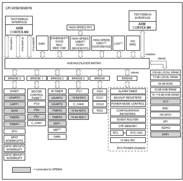
Figure 6: High-end dual core mixed-signal ARM processors let the smaller Cortex-M0 processor act as a coprocessor to the Cortex-M4 big brother with DSP extensions and floating point. Notice how multi-port DMA and multi-layer matrix bridges peripherals and resources (Courtesy of NXP Semiconductors).
Conclusion
There is a bounty of mixed-signal microcontrollers from which to choose that have basic and advanced features for data acquisition and sensor interfacing. If size and power matter, there are clever designs out there to use.
Common cores offer an easier migration path compared to a ground-up redesign, but expect to have a few snafus along the way with any design that preserves legacy code or architectural tricks. A performance increase in a core can upset delicate timings, so be careful with code migration. The key to success is matching the need with the best choice of processor.

免责声明:各个作者和/或论坛参与者在本网站发表的观点、看法和意见不代表 DigiKey 的观点、看法和意见,也不代表 DigiKey 官方政策。




 中国
中国