Microcontrollers for Low Energy Smart Power Applications
投稿人:DigiKey 欧洲编辑
2012-08-22
Microcontrollers are running at ever-lower power consumption to open up new applications such as smart lighting and wireless metering. New devices are pushing down power usage and giving engineers many more options in their designs, from high-level language development tools to the range of different peripherals.
The drive for smart power comes from a number of directions. Being able to monitor and control power consumption close to the point of load allows power to be more evenly spread across the grid and reduces waste power for the operator. For the user it can provide more flexible tariffs, lower power costs, and help to reduce the overall power usage, reducing costs even further. However, the equipment has to be cost effective, both in the capital costs and also in the maintenance. Replacing the batteries in millions of smart meters is a major operational cost for grid operators and a potential drawback for the implementation. Reducing the power consumption of the smart devices not only does what it says in reducing power consumption, but also allows batteries to run for many years.
Reducing power further through effective device management, new low power design architectures, and power-sensitive manufacturing processes can also bring the total power budget down to the point where no batteries are needed. At this point, energy can be harvested from the environment – often from vibrational or thermal energy in an industrial environment – and stored in a local battery. This provides power for a microcontroller and often a sensor and a network link for monitoring. The choice of architecture for the node and for the microcontroller is vital for the performance and the battery life, and there are several different options.
Design trade-offs
Integration and performance are all tied into the power considerations for microcontrollers used in smart power applications. A wide range of peripherals are available which can be added to a controller core to reduce the need to go off-chip and so reduce the power consumption. Sometimes, however, it can be more effective to use a small 8-bit controller alongside the wireless link than have a completely integrated system that tries to combine an applications processor with RF. While some controllers, such as the EFM32 developed by Energy Micro (below), have sophisticated power management that can switch off individual peripheral blocks to keep the power consumption to a minimum, having separate controllers can provide a way to isolate different parts of the node so that power is only used when absolutely necessary.
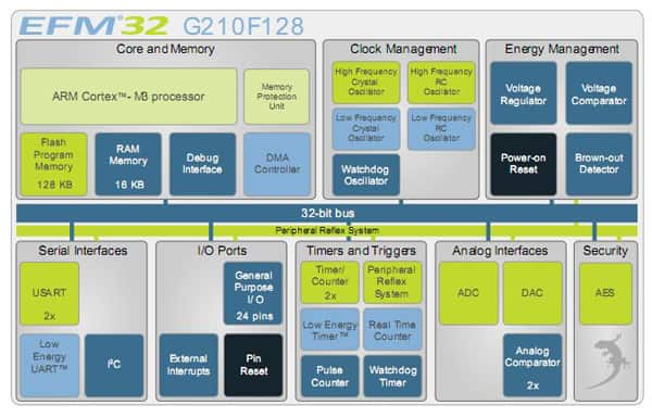
Figure 1: The EFM32 ‘Gecko’ low power core from Energy Micro.
There is also another trade-off between performance and power. Being able to use a power-efficient architecture quickly and then shut down the device can use less energy than using a slower, nominally lower power device for more time. However, this depends on the start-up and shut down times, but more devices are including this fast response in order to reduce power. Sometimes, though, the intricacies of the power management have little effect and the code size has more impact. Storing 16-bit or even 8-bit code can reduce the memory requirements and provide faster access, cutting cost and power. However, 32-bit systems are also able to take advantage of the smaller word sizes with reduced instruction sets such as ARM’s 16-bit Thumb 2.
In smart power, the software is not particularly complex but it does have to be extremely reliable – having to replace or update nodes with problems can be very costly. This means the existing legacy code is a valuable resource, and code reuse is a vital part of the design requirement. At the same time, the new generation of design tools and Integrated Development Environments (IDEs) for ARM MIPS and other 32-bit architectures allows faster development, higher quality code, and more efficient debugging, bringing a project to market faster and more reliably. This can influence the choice of microcontroller architecture.
All of this is the balance that designers are facing in developing smart power systems, and there are several approaches to implementing smart power, reflecting the tight design constraints of power and cost. Systems using 32-bit controllers, often around ARM’s power optimized Cortex-M3 core, are increasingly common.
Norwegian start-up Energy Micro has used the ARM Cortex M3 core to develop microcontrollers with the lowest energy consumption in the market, allowing long term battery use or even power from energy harvesting.
The EFM32G210F128 ‘Gecko’ uses low energy design with a short wake-up time from energy saving modes and a wide selection of peripherals to control smart power devices. The family of controllers is aimed at battery-operated applications for managing nodes in smart power networks.
At the heart of the chip is the Energy Management Unit (EMU) that handles all the low energy modes, switching peripherals on and off, as well as switching off the power to unused SRAM blocks to reduce power to a level of just 20 nA in the 3 V shutoff mode. There is a 0.9 µA Deep Sleep Mode that supports the Real Time Clock with 32.768 kHz oscillator, Power-on Reset, Brown-out Detector, RAM and CPU retention rising to 180 µA/MHz in the 3 V Run Mode with code executed from Flash.
The EMU makes use of a specially developed Clock Management Unit (CMU) that allows software to manage the individual clocks on the peripheral blocks that can consume significant amounts of power, even when not in use.
Energy Micro has also developed a Peripheral Reflex System (PRS) that lets the different peripheral modules communicate directly without involving the CPU. The peripheral modules that send out Reflex signals are called producers and the PRS routes these reflex signals to consumer peripherals that apply actions depending on the data received.
It also differentiates its Gecko microcontrollers with a Low Energy UART that allows two-way UART communication, on a strict power budget, at speeds of 9600 bit/s from a single 32.768 kHz clock. Similarly, a Low Energy 16-bit timer (LETIMER) can be used when most of the device is powered down, allowing simple tasks to be performed while the power consumption of the system is kept at an absolute minimum. The LETIMER can be used to output a variety of waveforms with minimal software intervention. It is also connected to the Real Time Counter (RTC), and can be configured to start counting on compare matches from the RTC.
Texas Instruments also uses the ARM Cortex M3 core for its Stellaris 1000 family of microcontrollers, aimed at the same battery powered, cost-conscious embedded smart power applications. The LM3S1000 series extends the family with larger on-chip memories, better power management and more I/O and control capabilities.
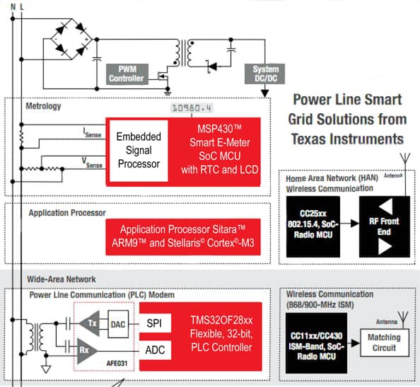
Figure 2: TI’s smart power implementation.
The LM3S1911 microcontroller is targeted at industrial applications, including remote monitoring, electronic point-of-sale machines, test and measurement equipment, network appliances and switches, factory automation, HVAC and building control, gaming equipment, motion control, medical instrumentation, and fire and security.
It has a battery-backed hibernation module to efficiently power down the device to a low-power state during extended periods of inactivity. Features also include a power-up/power-down sequencer, a continuous time counter (RTC), a pair of match registers, an APB interface to the system bus, and dedicated non-volatile memory.
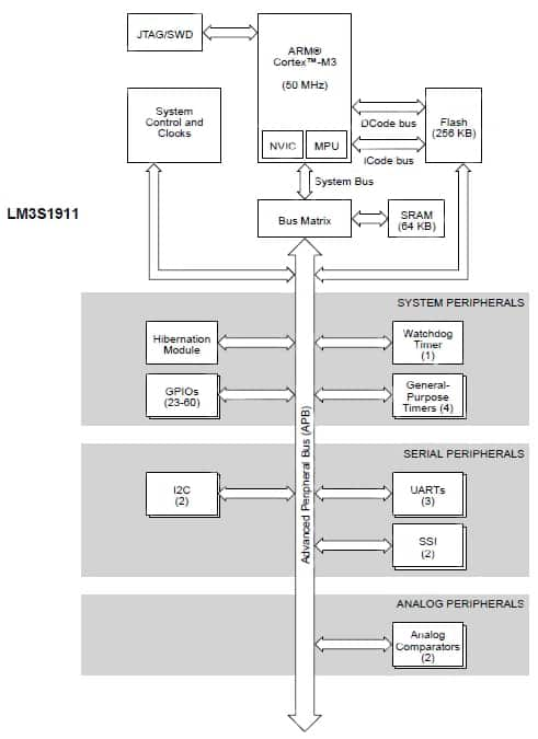
For linking to other parts of the system, the LM3S100 provides three fully programmable 16C550-type UARTs with IrDA support. These have separate 16 x 8 transmit (TX) and receive (RX) FIFOs to reduce CPU interrupt service loading and a programmable baud-rate generator, allowing speeds up to 3.125 Mbit/s. A programmable FIFO includes 1-byte deep operation to implement a conventional double-buffered interface.
16-bit is not dead
As shown by ARM’s Thumb-2 16-bit instruction set, there are advantages to the compact code, and some different architectural approaches can provide benefits for smart power designs. Microchip’s 16-bit DSPIC33EP256MU80 microcontroller adds a dedicated DSP block to a 16-bit core to get a similar effect with 60 MIPS of performance.
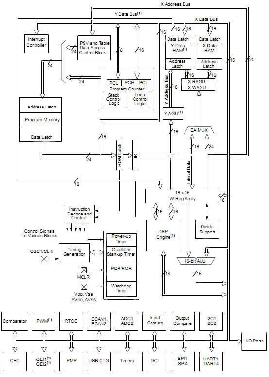
Figure 4: Microchip’s 16bit core with DSP accelerator.
It has a modified Harvard Architecture and, like the 32-bit and Thumb-2 code, uses a C Compiler with an optimized Instruction Set on its 16 bit-wide Data Path and 24 bit-wide execution pipeline. There are seventy-three base instructions, mostly with an effective instruction execution throughput of one instruction per cycle to provide added performance. The single cycle DSP MAC block provides support for eleven additional instructions with two 40-bit accumulators with rounding and saturation options as well as additional module and bit-reversed addressing modes.
A 15-channel Direct Memory Access (DMA) engine provides transfer of data to and from any data memory location with a dual-port DMA Buffer Area of up to 4 Kbytes to store data transferred via DMA. This provides fast data transfer between RAM and a peripheral while the CPU is executing code without having to use cycles from the execution core, improving the performance and reducing power.
Communication modules include a dual role USB v2.0 On-The-Go (OTG) block that are either Host or Peripheral in Low-speed (1.5 Mbps) and Full-speed (12 Mbps) mode. A high-precision PLL for USB supports up to thirty-two endpoints (sixteen bidirectional) and the USB module can use any RAM location on the device as USB endpoint buffers for the on-chip USB transceiver or as an interface for an off-chip transceiver.
8-bit lives as well
Even 8-bit cores are still being used effectively. Silicon Labs’ C8051F981-GM is an 8-bit pipelined 8051 core that has been optimized for very low power with a 150 µA/MHz active current from 1.8–3.6 V at 25 MHz and 25 MIPS. With a 2 µs wake up from sleep and a 1.5 µs analog settling time, the device can be ready quickly for making measurements or linking to a wireless network.
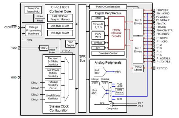
Figure 5: Silicon Labs’ C8051 8bit pipelined core.
The ADC provides 75 Ksamples/s with 12-bit resolution or 330 Ksamples/s with 8-bit resolution across ten channels. The device also includes a built-in temperature sensor.
Bridging the gap
Freescale is looking to bridge the gap between 8-bit and 32-bit capabilities with a series of Flexis devices that have a common set of peripherals and development tools to provide migration flexibility. The QE family, comprised of a pin-compatible 8-bit SO8 and 32-bit ColdFire V1 device duo, is the first family in the Flexis series and includes its lowest power MCUs. This is also the basis for other derivative low-voltage, low-power (LVLP) devices. The family is particularly aimed at consumer and industrial applications that require long battery life.
The MCF51QE128LH is a 32-bit controller based on the V1 ColdFire instruction set that extends the low end of the ColdFire embedded controller family with up to 128 KB flash memory and a 12-bit analog to digital converter (ADC) with up to twenty-four channels. The MCF51QE128 includes up to 3.6 V supply voltage, a 50 MHz CPU core, and three timers for improved motor control for industrial equipment including smart power, networked smoke detectors and security cameras.
The 32-bit MCF51QE128 is pin-, peripheral- and tool-compatible with the 8-bit S08QE128 device, providing design freedom across the performance spectrum. The ColdFire Instruction Set Revision C (ISA_C) provides additional instructions for easy handling of 8-bit and 16-bit data and support for up to 256 interrupt/reset sources for software flexibility and optimization of real-time applications.

Figure 6: The MC51QE128 32bit controller from Freescale Semiconductor is compatible with an 8-bit version.
There are two ultra-low-power (ULP) stop modes, one allowing limited use of peripherals while still sampling applications in a reduced power state which extends the battery life. There is also a new ULP power wait mode with a typical wake up time of 6 µs and an ultra-low-power OSC for accurate time-base in low-power modes.
There are two analog comparators with the option to compare to an internal reference. This means the output can be routed to a timer/pulse width modulator (PWM) block as the input capture trigger, requiring only a single pin for input signal and freeing up additional pins for other uses. The Analog Digital Converter (ADC) provides up to 24-channels with 12-bit resolution and a 2.5 µs conversion time, as well as a sensitive temperature sensor of 1.7 mV/°C.
The capabilities come from a low power process utilizing transistors with an increased channel length that reduces leakage current, which thereby decreases static power consumption. The standard cell library used to build the controller includes a very-low-power (VLP) oscillator that consumes only 500 nA, a low-dropout standby regulator that enables low-power running, and a wake up mode that takes just 6 μs, down from 110 μs previously. This all means an application can wake up, perform a task, and quickly go back to sleep to save additional power.
User-selectable peripheral clock gating enables energy-efficient optimization of the clock tree, which can consume up to 40 percent of the power used by the different modules, while a self-timeout block (SATO) allows the flash memory to be powered up long enough to perform a read with the result latched then automatically powered down. This process automatically kicks in at very low CPU rates and provides a much better current at low frequencies for flash operation.
Conclusion
The wide range of microcontrollers available for applications such as smart power can seem bewildering. However, there are a wide range of opportunities to optimize the system design for low power by selecting the right combination of peripherals and capabilities within the power budget. The developments in process technology and ultra-low-power circuit design mean that many devices can now be used for designs that aim to have a ten-year battery life or even use energy harvesting to eliminate maintenance costs. With increased integration to reduce the overall cost of the bill-of-materials, the implementation of smart power systems becomes viable in helping to reduce power all the way from the factory floor to the enterprise.

免责声明:各个作者和/或论坛参与者在本网站发表的观点、看法和意见不代表 DigiKey 的观点、看法和意见,也不代表 DigiKey 官方政策。




 中国
中国