Microcontroller Systems for Sensor Control and Interface
投稿人:Convergence Promotions LLC
2013-04-17
Microcontrollers are becoming the core engine for sensor-based systems in both industrial and commercial systems. The ability to create a core platform and implement only low cost software and firmware-based changes for sensor applications has driven the rise in the availability and diversity of development boards. While primarily interfacing through serial ports, analog and mixed-signal sensors influence the performance of the microcontroller, the OS selection, and the power/performance of overall design. The use of application-specific development boards simplifies design tasks and helps to finalize designs in a timely manner.
Sensor control and interface
Embedded systems are increasingly using multiple sensors to sample their environment. A large number of these sensors use simple serial interfaces that produce digital output, which can be directly processed by the microcontroller. Some of these systems use traditional serial interfaces that are multiplexed among the sensors to provide the controllers with the structure to handle just one input at a time (GPIO, I²C, SPI, RS232, RS422, etc.). Other serial sensor devices incorporate full protocol management of the USB interface and that interface's methods for multi-device management.
While communication with sensors is digital, most sensors are analog. Analog sensors include light and IR detectors, thermocouples, touch controllers, sound and external-area motion sensors, device position and movement sensors, and temperature and pressure sensors. The resolution and accuracy levels of analog sensors dictate not only the size of the data stores and word size but also the speed and math processing capabilities of the MCU.
Since there many different types of sensors, the primary method for system development involves selecting a core controller and then programming in software an application that calls an interface software routine for the specific sensor being used. Using this approach, the designer can create a common design platform and GUI while leaving the final optimization step for a particular sensor and application until the very end of the design cycle. Most of the MCU software development kits (SDKs) are designed to support this methodology and include development boards that are optimized for this approach.
Optimized data acquisition systems
As most of the sensors being used today are analog, standard product data acquisition systems such as the ADUC7060 (see Figure 1) from Analog Devices, which brings high-performance signal paths to the standardized ARM7™ core MCU. These single-chip solutions are multi-featured and designed to address the high sensor count industrial application space.
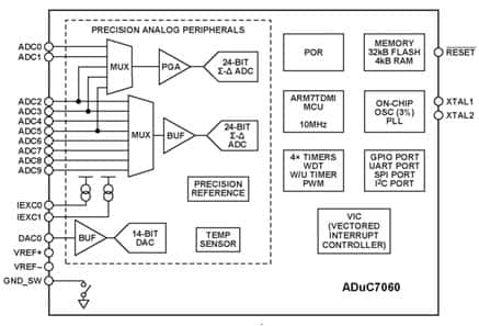
Figure 1: Analog Devices’ ADUC7060 block diagram. (Courtesy of Analog Devices.)
Analog Devices’ ADuC7060 is a fully integrated, 8 ksps, 24-bit data acquisition system incorporating high-performance multichannel sigma-delta (Σ-Δ) analog-to-digital converters (ADCs), plus an on-chip oscillator and a PLL that generates an internal high-frequency clock up to 10.24 MHz. The MCU core is an ARM7TDMI, 16-bit/32-bit RISC machine offering up to 10 MIPS peak performance; 4 kB of SRAM; and 32 kB of nonvolatile Flash/EE memory, all provided on-chip. The ARM7TDMI core views all memory and registers as a single linear array.
The data acquisition and sensor interface subsystem consists of a 5-channel primary ADC and up to an 8-channel auxiliary ADC. The ADCs operate in single-ended or differential input modes. A single channel buffered voltage output DAC is available on-chip. The DAC output range is programmable to one of two voltage ranges.
Since the device is designed for real-time sensor interface and signal interpretation, the ADuC7060 contains an advanced interrupt controller. The vectored interrupt controller (VIC) allows every interrupt to be assigned a priority level. It also supports nested interrupts to a maximum level of eight per IRQ and FIQ. When IRQ and FIQ interrupt sources are combined, a total of sixteen nested interrupt levels are supported. On-chip factory firmware supports in-circuit serial download via the UART serial interface ports and non-intrusive emulation via the JTAG interface. The parts operate from 2.375 to 2.625 V over an industrial temperature range of −40°C to +125°C.
Digital interface sensor and controller development options
In addition to the analog interface that requires a data acquisition module, there is also the traditional serial data interface that appears in SPI, RS232, and USB formats. Evaluation and development systems like the MSP-EXP430FG4618 Experimenter Board from Texas Instruments are designed for common digital inputs and one to two analog sensor applications. Figure 2 shows the evaluation board with an embedded capacitive touchpad. Figure 3 shows the functional block diagram for the design.
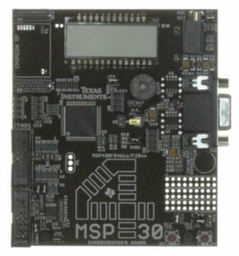
Figure 2: TI’s MSP-EXP430FG4618 Experimenter Board with touch sensor (Courtesy of Texas Instruments).
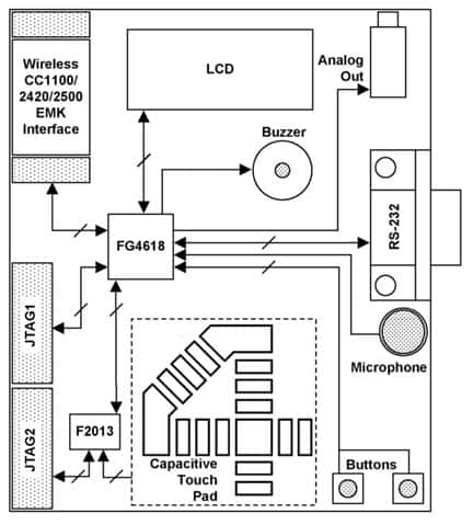
Figure 3: TI’s MSP-EXP430FG4618 Experimenter Board functional block diagram (Courtesy of Texas Instruments).
Optimized for external digital interfaces, the experimenter board features typical modules needed for most embedded control applications. These modules include a 4-Mux LCD display, two momentary-on push button switches, four LEDs that can be used for display purpose for status of which two can be jumpered off for lower power applications, a buzzer that runs from a digital I/O port, a “4” shaped capacitive touch pad that is connected to the digital I/O ports for single touch sensing, an RS-232 port with UART; and an I²S/SPI connection for inter-processor communications through the two JTAG ports. On the analog side, there is a microphone that outputs to a set of analog filters, data converters, and an active LPF and buffer amplifier driving the analog output. This analog signal chain is shown in Figure 4. Finally, the board contains multiple sets of clock sources including a crystal oscillator.
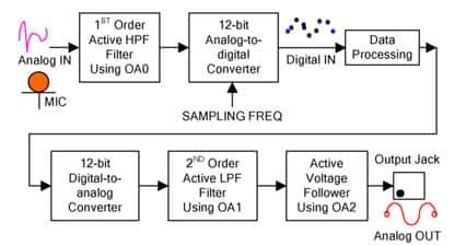
Figure 4: TI’s MSP-EXP430FG4618 Experimenter Board analog signal path (Courtesy of Texas Instruments).
The board is designed to have a central processing block that is software programmed to manage the embedded system application. The direct digital inputs reach the processor directly and utilize the interrupt controller. The same core digitally processes the signals from the analog path shown in Figure 4 after conversion from the analog domain. This evaluation/development board can be used as a platform for multiple projects since the interface code and overhead for turning on the system functions are independent of the end application. This allows a software core module to address a common GUI and development methodology so that media control, industrial control, robotics, and environmental control systems can all be designed with the same flow.
Extending wireless development
While the MSP430FG4618 targets multiple sensor control in the core processor path, Texas Instruments’ eZ430-RF2500 development kit is a USB-based wireless development product that uses the same MSP430 application development software. The kit is a complete wireless development tool providing all the hardware and software to evaluate the MSP430F2274 microcontroller and CC2500 2.4 GHz wireless transceiver.
The eZ430-RF2500 uses the IAR Embedded Workbench® IDE or TI’s Code Composer Essentials (CCE) to write, download, and debug an application. The debugger is unobtrusive, allowing the user to run an application at full speed with hardware breakpoints while at the same time providing single-stepping capability and consuming no additional hardware resources.
TI’s eZ430-RF2500T target board is an out-of-the-box wireless system that may be used with the USB debugging interface to a PC, as a stand-alone system with or without external sensors, or it may be incorporated into an existing design. The new USB debugging interface enables the eZ430-RF2500 to remotely send and receive data from a PC using the MSP430 application UART.
The eZ430-RF2500 (see Figure 5) features a USB debugging and programming interface with a driverless installation and application back channel, a total of 21 available development pins for external connections, an ultra-low-power MSP430 MCU with 16 MHz performance, two general-purpose digital I/O pins connected to green and red LEDs, and an interrupt pushbutton for user feedback.
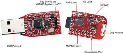
Figure 5: TI’s eZ430-RF2500 USB wireless development kit. (Courtesy of Texas Instruments.)
This wireless-optimized MSP430 design incorporates a chip antenna and full wireless system, as well as an analog sensor subsystem with common software control. The analog sensor subsystem includes a 200 ksps 10-bit SAR ADC, two built-in operational amplifiers, a watchdog timer, 16-bit Timer_A3 and Timer_B3, a USCI module supporting UART/LIN, SPI, I²C, or IrDA interfaces, and software control of low-power modes, resulting in a current drain of as little as 700 nA in standby mode.
The eZ430-RF2500 development kit comes with a CD that includes two different development software tools for the MSP430: IAR Embedded Workbench KickStart and Code Composer Essentials (CCE). The KickStart version is a reduced memory subset of the full CCE tool. The CCE tool is available for purchase for use with any MSP430 family MC.
High-speed connectivity development
Following the trend toward unified development for multi-sensor and multi-input systems, Zilog has updated their core Z80 processors to a single board computer (SBC) system in a connectivity optimized ASSP. The EZ80F917050SBCG (see Figure 6) is an implementation of Zilog’s Zdots® SBC for eZ80AcclaimPlus!™ Connectivity ASSP. Unlike traditional development systems, this one is optimized for media and internet/intranet control and data processing.
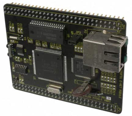
Figure 6: Zilog’s Zdots SBC for the eZ80AcclaimPlus! ASSP. (Courtesy of Zilog.)
The SBC for the connectivity ASSP features a 10/100 Base-T Ethernet PHY with RJ45 connector, 512 KB of fast SRAM along with a 256 KB on-chip Flash memory, a 1 MB off-chip NOR Flash memory, a battery-backed real-time clock; an input/output connector with 32 general-purpose 5V-tolerant I/O pins, and Zilog’s ZHX1810 IrDA transceiver. An onboard connector provides external peripheral connections (IRQ, CS, 24 address, and 8 data) to the I/O bus as well as providing a low-cost connection to carrier board via two 2x30-pin headers and a 3.3 V power supply.
Like the TI parts, the Zilog ASSP features internal Flash memory, multiple low-power modes, two independent UARTS, I²C and SPI interfaces with independent clock generators, an IrDA-compliant infrared encoder/decoder, a real-time clock with on-chip oscillator, four 16-bit counter/timers, a watchdog timer, JTAG and ZDI debug interfaces, and 32 bits of GPIO. The main differences include the 10/100 Mbps Ethernet MAC with an 8 KB frame buffer and a single-cycle instruction-fetch pipelined eZ80 CPU core. Figure 7 shows the block diagram of the ASSP.
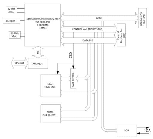
Figure 7: Zilog’s eZ80AcclaimPlus! ASSP functional block diagram. (Courtesy of Zilog.)
The architecture of the eZ80 core and the general application of the SBC require the inclusion of the fast buffer. The fast buffer exists to prevent bus contention that occurs because of the timing difference between the slow turn-off time of the module’s external Flash and the fast bus turn-around time of the eZ80F91. The problem related to bus contention when using eZ80 family of the microprocessors in NATIVE eZ80 mode is well documented in the development kit and product specification for the eZ80F91.
Bus contention occurs when two or more devices drive a common bus such as the multiple GPIO channels, the UARTs, or the Ethernet controller. Some of the external devices are slower than the native single-cycle execution time of the eZ80F91. This can result in the Flash turn-off time being three to four times longer than the bus cycle time, which in turn results in the Flash output drivers going into High-Z mode. That would cause the eZ80F91 Read access to Flash to take the sum of the CPU cycle time plus the Flash turn-off time to be the active time before Flash stops driving the data bus. At this point the eZ80F91 device is already well into the next bus cycle, resulting in data contention. Since there is a mix of high-speed Ethernet traffic, as well as standard low speed sensor signals on the bus, and since sensor traffic is asynchronous, the SDK and the board have to allow for the insertion of the fast buffer to address this issue.
The general platform development methodology described in this article requires a unified software code base as well as an application development board that can address multiple external sensors. These sensors have a variety of interfaces, both analog and digital. These interfaces range not only in the size and precision of the data being sent, but also in the speed. Control and adjustment of the timing of the systems while maintaining a common GUI, application interface, and acquired data stored in software is key to developing multiple products from a single MCU base.
Summary
As sensor-based systems increase in functionality, the incorporation of embedded microcontrollers is becoming a dominant trend. These devices, with their ability for in field programming of both firmware and software, are the basis for system design. These systems use a combination of FPGA-based core microcontrollers and low-power stand-alone microcontrollers at the heart of the system. However, sensors and the Internet of Things (IOT) world require signal-processing applications, and as a result, they require real world testing in form-factor appropriate design prototypes to check their real-time aspects and the signal integrity of the design. Most vendors and numerous third party partners have created microcontroller-based development systems that are available along with SDKs as are the core processor components.

免责声明:各个作者和/或论坛参与者在本网站发表的观点、看法和意见不代表 DigiKey 的观点、看法和意见,也不代表 DigiKey 官方政策。


