Maxim’s Smart Force Sensor Reference Design: MAXREFDES82#
2016-09-29
Introduction
Technology marches forward, constantly and irrepressibly altering the world of human-to-device interfaces. From mobile device touchscreens to weigh scales with electrodes for body composition, machines continue to add more capability and different ways to gather their measurements. Every so often, a truly elegant concept emerges, merging technology, design and simplicity. The Maxim MAXREFDES82# is one such elegant concept.
This reference design is an industrial, smart force sensor. The design measures mass as well as the center of mass of the object on it. This combination of features and speed means that the MAXREFDES82# operates as both a weigh scale and a touch interface with force sensing. Built with a plastic plate, the system ideally meets the needs of industrial human machine interfaces (HMI).
The reference design features the MAX11254 24-bit, 6-channel, 64 ksps delta-sigma ADC with SPI interface. Four load cells are mounted on a quadrant plane to detect touch forces applied on the flat plastic plate. Based on the forces applied on each individual load cell, the system displays the total force magnitude and the coordinates of the force center. The force magnitude and coordinates are scanned approximately each 10 milliseconds.
The system includes a thin-film-transistor (TFT) liquid crystal display (LCD) module, digitally showing the forces on each individual load cell and the total force applied on the top plate. The LCD module also graphically displays the force magnitude and the coordinates of the force center.
The MAXREFDES82# reference design consumes minimal energy and is powered by a USB port. A PC-side graphical user interface (GUI) program is also included to facilitate the human interface input demonstration and development.
The reference design block diagram of the MAXREFDES82# (Figure 1) demonstrates how a touch force and its movement are captured and used in a 3-dimensional (3D) human-interface input device. The design includes source files for the microcontroller to enable developers to quickly evaluate and customize the design for their specific applications with minimal firmware or hardware changes. The board is designed in a compact form factor for rapid evaluation or installation.
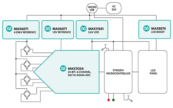
Figure 1: MAXREFDES82# reference design block diagram.
Detailed Description of Hardware
Figure 1 shows the MAXREFDES82# reference design system block diagram. Figure 2 shows the assembly view of the design. Also refer to the schematic for circuit details.
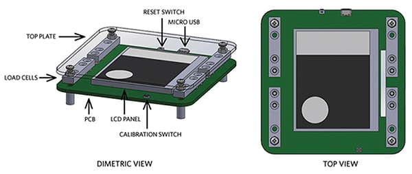
Figure 2: MAXREFDES82# reference design assembly views.
When a touch force or weight contacts the surface of the top plate, the four strain-gauge load cells deform and send electrical signals to the MAX11254 ADC. Based on the distribution of the force to the four load cells, the system calculates the total force and the position of the force's center of mass. The system continuously scans the signal output of each of the four load cells, and an accurate force and its movement map can be acquired. Because the system gathers and monitors not only the force position, but also the force magnitude, the system is ideal for a 3D human interface input application.
The reset switch (SW1) resets the board, and the calibration switch is used to start a calibration procedure.
The red light-emitting diode (LED) indicates the power supply is good. The flashing green LED indicates the ADC is converting.
MAX11254 24-Bit, 6-Channel, 64 ksps, Delta-Sigma ADC with SPI Interface
The MAX11254 IC lies at the center of the system. The device is a 6-channel, 24-bit delta-sigma ADC that achieves exceptional performance while consuming very low power. Sample rates up to 64 ksps allow precision DC measurements. The MAX11254 communicates through an SPI serial interface and is available in a small (5 mm x 5 mm) TQFN package.
The device offers a 6.2 nV/√Hz noise programmable gain amplifier (PGA) with gain settings from 1x to 128x. The integrated PGA provides isolation of the signal inputs from the switched capacitor sampling network. The PGA also enables the IC to interface directly with high-impedance sources without compromising available dynamic range.
The device operates from a single 2.7 V to 3.6 V analog supply, or split ±1.8 V analog supplies, allowing the analog input to be sampled below ground. The digital supply range is 1.7 V to 2.0 V, or 2.0 V to 3.6 V allowing communication with 1.8 V, 2.5 V, 3 V, or 3.3 V logic.
In this smart force sensor design, the MAX11254 is configured as follows:
- VAVDD = 3.6 V, VAVSS = 0 V, VDVDD = 3.6 V, VREFP - VREFN = 1.8 V
- ADC sampling rate = 200 sps
- PGA gain = 128
- Single-cycle conversion mode (SCYCLE = 1)
- Sequencer mode = 2
- Channel map = CH0, CH1, CH2, Ch3
- MUX delay = 1024 µs
The developers can easily change the configurations to their specific requirements in the provided firmware.
Strain-Gauge Load Cells
The strain-gauge load cells are excited by a 4.096 V reference. When the strain-gauge load cells are deformed by the load acting on them, the load cell electrical resistances change, hence the load cell outputs a voltage change proportional to the load.
For the touch application, the design features load cells from Phidgets Inc. The load cell capacity is 780 g with a rated output of 0.8 mV/V. The non-linearity is 0.05% FS, non-repeatability is 0.05% FS, and the temperature effect on span is 0.05% FS. Depending on the specific application and accuracy requirement, different load cells can be selected and replace the load cells mounted on the board.
One caution to note, do not overload the load cells for more than 10 seconds.
Power Supplies and Voltage References
A micro-USB cable connected to a PC powers the MAXREFDES82#.
- The MAX17651, ultra-low quiescent current, linear regulator (LDO) regulates the 5 V input to 3.6 V
- The MAX6071 4.096V output, low-noise, high-precision series voltage reference excites the load cells
- The MAX6071 1.8V output voltage reference drives the MAX11254 ADC reference
- The MAX8574 high-efficiency step-up converter generates the nominal 19.2 V LCD module back lighting power supply
Microprocessor and the LCD Module
The MAXREFDES82# reference design uses STM32F429 as the processor. The processor controls the ADC, the LCD module, and performs all computations. The TFT LCD module measures 3.5” across the diagonal with a resolution of 240 x 320 pixels. In this design, the upper section of 240 x 120 pixels digitally displays the load cells load information, the lower section of 240 x 240 pixels graphically displays the force magnitude and its relative positions in the square constructed by the four load cells.
Firmware Description
The MAXREFDES82# firmware is based on an interrupt-driven design model. After power-up, the microprocessor configures the power domains, clock domains, LCD module controller, USB stack, virtual COM port (VCP), and other house-keeping tasks. Then the microprocessor enters into a loop, scanning the load cells and processing the data. The results are displayed on the LCD panel. The results can also be displayed on a PC GUI application. The GUI application communicates with the board through VCP communication.
Figure 3 shows the MAXREFDES82# firmware main function flowchart. Refer to the source files found on the Maxim website for firmware details.
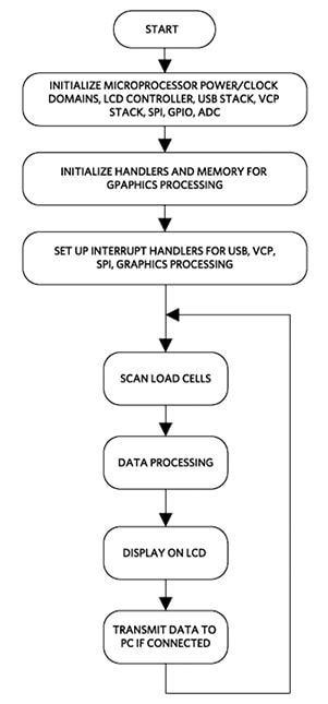
Figure 3: MAXREFDES82# firmware main function flowchart.
GUI Application Description
The MAXREFDES82# board can work alone without the PC GUI application. However, the GUI application does conveniently provide results on a PC screen.
Figure 4 shows the MAXREFDES82# GUI application screenshot. Before connecting the MAXREFDES82# board to a PC USB port, the user should install the STMicroelectronics VCP driver. See the Quick Start Guide section below for details.
When the reference design board receives power and finishes the power-up calibration, the board is in measurement state. Run the GUI application and click Connect button, the PC GUI displays the same information as the information displayed on the LCD panel.
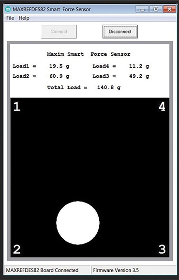
Figure 4: MAXREFDES82# GUI application screenshot.
Quick Start Guide
Required Equipment:
- MAXREFDES82# reference design board
- A PC with a spare USB port and a micro-USB cable
Follow the ensuing procedure to verify the correct functioning of the MAXREFDES82#.
Procedure
- Run the proper virtual COM port driver .exe file included in MAXREFDES82SW10.zip. For a 32-bit windows machine, run VCP_V1.3.1_Setup.exe, for a 64-bit windows machine, run VCP_V1.3.1_Setup_x64.exe.
- Connect the MAXREFDES82# board to the PC with the USB cable. Wait for the PC to complete the driver installation.
- Follow the instructions on the MAXREFDES82# board LCD screen to finish the power-up calibration.
- After the power-up calibration is done, the board is in measurement state.
- Run MAXREFDES82SW10.exe file included in MAXREFDES82SW10.zip.
- Click Connect button on the PC GUI, the PC GUI should display the same information as board LCD screen.
- Test the touch screen with forces less than 570 grams. The board can be temporarily overloaded up to 2 kilograms of force.
- When the PC GUI is in a connected state, don't disconnect the USB cable or press the SW1 reset switch on the MAXREFDES82# board. Disconnect the cable or press the SW1 reset switch only when the PC GUI is in the disconnected state, or when the PC GUI application is not running at all.
Lab Measurements
The MAXREFDES82# design is verified and tested under typical application cases. The platform is targeted for any developer who uses the MAX11254 24-bit, multi-channel ADC to capture high precision analog signals in weigh scale and touch applications. The reference design is flexible enough to be customized for specific applications development, e.g., weigh scale applications, industrial control and automation application, etc.
Figure 5 shows the weight measurement of a standard weight-set placed on the center of the top plate.
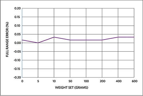
Figure 5: MAXREFDES82# full-range weight error for weight-set in the plate center.
Figure 6 shows the relative X-axis error of a standard weight-set placed on the center of the top plate.
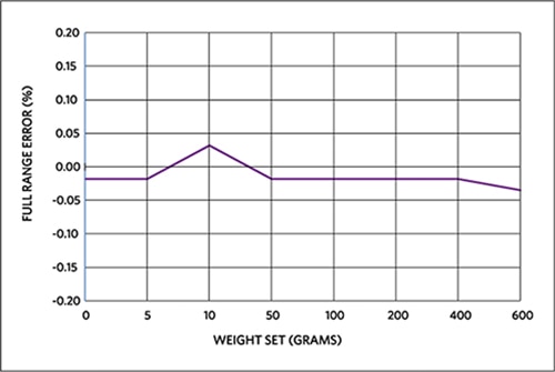
Figure 6: MAXREFDES82# full-range X-axis error for weight-set in the plate center.
Figure 7 shows the relative Y-axis error of a standard weight-set placed on the center of the top plate.
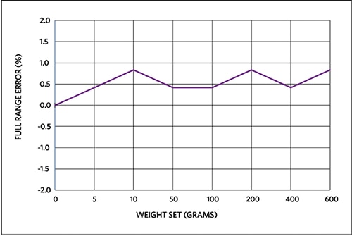
Figure 7: MAXREFDES82# full-range Y-axis error for weight-set in the plate center.
Figure 8 shows the weight measurement of a standard weight-set placed on the center of the top left quadrant of the top plate.
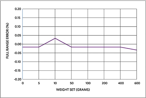
Figure 8: MAXREFDES82# full-range weight error for weight-set in the top left quadrant.
Figure 9 shows the relative X-axis error of a standard weight-set placed on the center of the top left quadrant of the top plate.
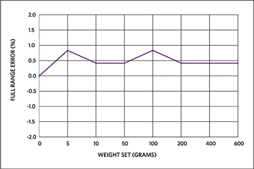
Figure 9: MAXREFDES82# full-range X-axis error for weight-set in the top left quadrant.
Figure 10 shows the relative Y-axis error of a standard weight-set placed on the center of the top left quadrant of the top plate.
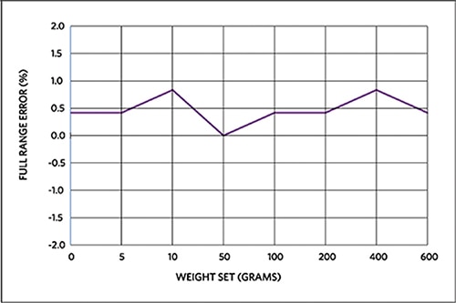
Figure 10: MAXREFDES82# full-range Y-axis error for weight-set in the top left quadrant.
免责声明:各个作者和/或论坛参与者在本网站发表的观点、看法和意见不代表 DigiKey 的观点、看法和意见,也不代表 DigiKey 官方政策。


