Integrated Phase-Locked Loops Offer Higher-Frequency Performance, Enhanced User Benefits
投稿人:电子产品
2015-11-12
The phase-locked loop (PLL) is one of the most versatile, flexible, and valuable circuit configurations in electronic systems, resulting in its use in many applications. It is used for clock retiming and recovery, as a frequency synthesizer, and as a tunable oscillator, to cite just a few examples. As a result, the PLL is found in a great many RF equipment items including radio receivers and test equipment. Depending on its specific implementation, it can serve from near-DC to GHz and higher frequencies, fulfilling many critical roles in systems and circuits.
The PLL is a closed-loop (negative feedback) architecture, and a basic PLL consists of these blocks (Figure 1):
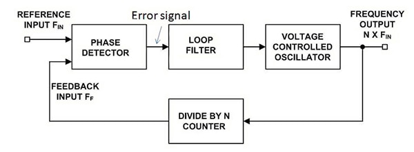
Figure 1: A basic PLL is a closed-loop, negative feedback system where the error between a reference signal and the VCO output is used to correct that output; the low-pass filter is a critical element in establishing the loop’s dynamics.
- A phase/frequency detector (PFD) (often simply called a phase-detector PD) compares an input signal to a reference signal and produces an error signal which is proportional to their phase difference (keep in mind that phase and frequency are intimately related, as frequency is the time derivative of phase); the phase-detector output usually goes to a charge pump which transforms the small current difference into a larger voltage
- A low-pass filter (LPF), which shapes the spectrum of the error signal; the design of this filter is often a combination of engineering science and intuitive art, and is a major factor in setting many of the dynamics of PLL operation
- A voltage-controlled oscillator (VCO) with output phase/frequency controlled by the error signal
- An optional frequency divider at the VCO output, which causes the PLL to generate frequencies at a multiple factor N of the reference frequency; N can be an integer, and many PLL designs support fractional-N non-integer division
The output of the VCO (and divider, if used) goes to the phase/frequency detector to complete the feedback loop. In operation, the error signal increases as the phase difference increases. This drives the VCO phase in the opposite direction, which reduces the error signal. As a result, the phase of the output is locked to the phase at the other input.
When the PLL output is closely tracking the input and the error signal is small and relatively stable, the PLL is said to be in “phase lock” or simply “lock.” Depending on the application, the output of the PLL system used in the system is either the output of the VCO or the control signal to the VCO.
PLLs were originally devised around the 1920s using vacuum tubes, of course. Their popularity expanded significantly with the introduction in the 1970s of the first mass-market PLL as an IC, the Signetics NE565, for 0.001 Hz to 500 kHz operation. Although this part is obviously now obsolete (and Signetics is long gone), its datasheet is archived and available online1.
PLLs can be built using analog, digital, or mixed-signal circuitry. Early PLLs were all-analog, with an analog phase detector, low-pass filter, VCO, and optional frequency divider; the divider was soon upgraded to a digital divider to allow integer and fractional-integer division. Digital PLLs now replace the phase detector with an up-down counter which performs an analogous function but in the digital domain, and may also use digital filters, with the error signal driving a direct-digital synthesizer as the VCO.
Due to the modularity of its internal structure, widespread use, and widespread applications, the PLL is the engineering counterpart to the works of Shakespeare or James Joyce, in that it has been the topic of countless articles, papers, and books. These have analyzed the PLL extensively with both broad qualitative discussions as well as highly detailed quantitative models; nearly all such analyses begin with the classic books by Gardner and Viterbi2,3.
Available technical papers cover the performance of the PLL with many kinds of noise, jitter, drift, nonlinearities, distortions, and other circuit imperfections in each of its functional blocks, as well as performance with many types of input signals. Among them are papers which examine the PLL operation in both time and frequency domains; some focus on simple first-order models while others use highly complex models which capture many real-world subtleties of the PLL circuitry and signals.
PLL parameters meet application goals
As with most electronic circuits, there are some basic parameters which apply to almost all applications and some that are more critical in specific cases. By adjusting some of the design specifics of the phase detector, low-pass filter, VCO, and divider, the PLL design can trade off performance across these parameters to best fit the application priorities. Among the top-level factors are:
- Operating frequency: the nominal, free-running frequency of the PLL and its VCO
- Operating range: the frequency span over which the PLL and VCO will operate. This includes the pull-in range over which the PLL can acquire a signal and achieve lock, as well as the wider range over which it can maintain lock once achieved
- Slewing or capture time: the time it takes the PLL to acquire and lock in to a signal at the outer limit of operation, determined in large part by the low-pass filter; a narrower-bandwidth filter has longer capture time but limits noise and jitter, while a wider-bandwidth filter has faster response but allows more noise to get through the PLL system
- Noise and jitter: any noise or jitter added by the PLL’s elements and which thus appear at its output, even with perfect signals. The overall noise figure of merit (FOM) is expressed in dBc/Hz, and there are several different types of FOM
- Deadband: when the two inputs to the phase/frequency detector are very close, the detector may not see this and therefore not produce an error output; this is somewhat analogous to electronic hysteresis or mechanical stiction
Many other factors may also apply to PLLs in different applications, such as spur-free dynamic range (SFDR), distortion, intercepts, and temperature coefficients; the full list can be quite lengthy.
PLL ICs moving up in frequency, performance, integration
In order to achieve the best mix of performance factors for a given application, users of PLLs would buy and connect separate blocks: phase/frequency detector, tailored filter, VCO, and other elements. Of course, makers of modules and hybrid devices soon offered complete PLLs as fully characterized units, by combining multiple individual IC die and discrete components.
However, the demand for wireless systems at higher frequencies, such as for software-defined radio, smartphones, radar systems, and many other applications, has been an incentive for IC vendors to develop processes and designs which result in high-performance monolithic PLLs. Many of these integrate most or all functional blocks (depending on frequency and needed performance) which reduce design-in time, risk, board real estate, and power dissipation.
For example, the HMC830LP6GE PLL from Hittite (now part of Analog Devices) is a fractional-N PLL for operation from 25 MHz to 3 GHz. It targets cellular/4G infrastructure, repeaters and femtocells, and communications test equipment, among other applications with ultra-low in-band phase noise of -110 dBc/Hz, a FOM of -227 dBc/Hz, and rms jitter below 180 fsec.
This IC includes an integrated VCO (Figure 2), which traditionally has been the most difficult function to integrate while still achieving high overall performance at high frequency. As with most PLLs, the data sheet has well over a dozen detailed graphs showing performance of many aspects of the PLL under a wide variety of conditions. Figure 3 shows the integrated rms jitter over the PLL’s operating range at various temperatures.
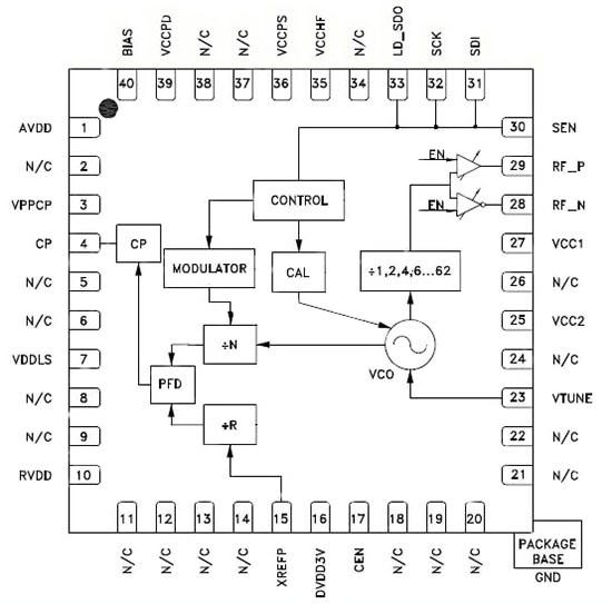
Figure 2: The HMC830LP6GE from Analog Devices is representative of a trend of the last few years: putting the VCO in the IC with the rest of the PLL, while also extending frequency range and without compromising the figure of merit.
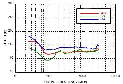
Figure 3: PLL data sheets typically have many performance graphs, such as this one for the HMC830LP6GE which show rms jitter (fsec) versus frequency, at -40⁰C, 27⁰C, and 85⁰C; note the performance stability across that wide range.
Another PLL with an integral VCO is the LTC6948 from Linear Technology Corp., a 370 MHz to 6.39 GHz fractional-N device also with ultra-low noise. It also includes a reference divider, phase/frequency detector, charge pump, fractional feedback divider, and VCO output divider. The normalized in-band phase-noise floor FOM is -226 dBc/Hz, and the wideband output phase-noise floor is –157 dBc/Hz (Figure 4).
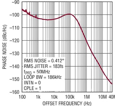
Figure 4: Among other parameters, the data sheet of the LTC6948 from Linear Technology includes the normalized in-band phase-noise floor FOM and the wideband output phase-noise floor; the latter goes from –100 dBc/Hz down to –157 dBc/Hz at highest frequencies.
It supports a reference input frequency up to 425 MHz, for fast-frequency switching. The IC is well-suited for applications such as wireless base stations (LTE, WiMAX, W-CDMA, PCS); microwave data links, and military/secure radios, and it can be used as the core of a high-speed, tunable 6.39 GHz wideband receiver (Figure 5).
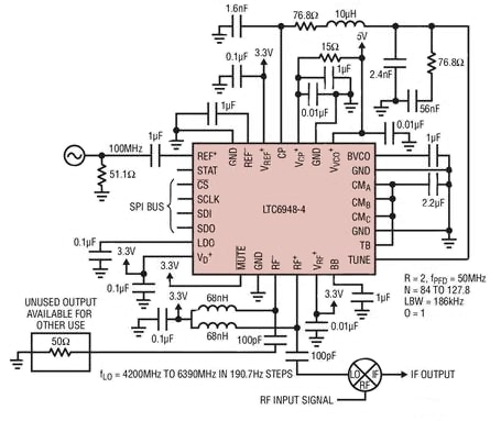
Figure 5: Even highly integrated ICs need passive-component support, as this schematic for a high-speed, tunable 6.39 GHz wideband receiver based on the LTC6948 indicates.
Maxim Integrated’s MAX2870 is a 23.5 MHz to 6 GHz PLL with fractional/integer-N synthesizer and VCO (Figure 6). The device achieves its ultra-wide frequency via multiple VCOs covering 3 GHz to 6 GHz, which can be selected automatically or under user control (via a serial interface); the user supplies the loop filter and reference. The phase/frequency detector operates to 105 MHz in Integer-N mode and 50 MHz in fractional-N mode, and accepts reference frequencies up to 200 MHz. The PLL shows excellent 6.0 GHz phase-noise performance across multiple divider settings (Figure 7). Applications include wireless infrastructure, test and measurement, satellite communications, and wireless LANs.
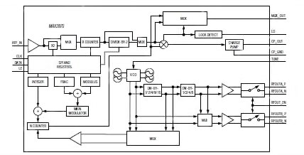
Figure 6: The MAX2870 from Maxim Integrated achieves its 6 GHz rating through the use of multiple internal VCOs, which can be selected automatically or by user initiative.
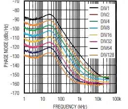
Figure 7: Again, PLL vendors provide detailed performance specifications such as this plot of phase noise for the MAX2870 across the operating bandwidth, with different division factors.
Although the Texas Instruments LMX2492 fractional PLL (Figure 8), does not include an integral VCO, it does operate from 500 MHz up to 14 GHz with an external VCO; its FOM is -227 dBc/Hz. When combined with a suitable loop divider, it can be used as the core of a 77 GHz automotive radar system (Figure 9); it also includes ramp/chirp generation for this focused application.

Figure 8: The Texas Instruments LMX2492 PLL does not include a VCO, but reaches 14 GHz performance with a FOM of -227 dBc/Hz.
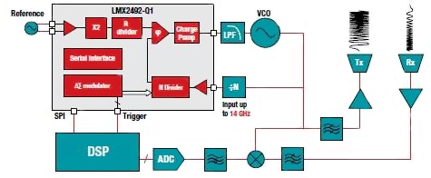
Figure 9: The LMX2492 targets applications such as 77 GHz auto radar, with integral ramp and chirp functions which radar requires.
Due to its 200 MHz phase-detector response, this PLL can also be used in non-radar applications such as mobile wireless, compact RF, radar modules, microwave backhaul, oscilloscopes, spectrum analyzers, land mobile radios, and software-defined radios. Despite its high-frequency rating, the IC operates from a 3.15 to 3.45 V supply and dissipates just 60 mA.
In addition to their RF performance, many PLLs now include SPI or I2C serial interfaces so the system processor can set and change some of the PLL parameters such as gain, filter bandwidth, or range. This enables the software to adjust these factors in a given circuit to meet changing scenarios, or allows the same component to be used across multiple designs.
Summary
The PLL has been a critical part of many electronic systems for communications, synthesis, clocking, signal generation, and signal-recovery applications for many decades. New ICs are pushing the performance specifications to new levels in terms of frequency, noise, and jitter performance, while integrating more features into a single device. By adding digital functionality, either within the loop design itself, or as a controlling feature for establishing PLL operating points, the versatility and flexibility of the PLL is even further enhanced.
For more information about the parts discussed in this article, use the links provided to access product pages on the DigiKey website.
References:
- Signetics NE565 datasheet
- Gardner, Floyd M. (2005), Phaselock Techniques (3rd ed.), Wiley-Interscience, ISBN 978-0-471-43063-6
- Viterbi, Andrew J., Principles of Coherent Communications, McGraw-Hill.
免责声明:各个作者和/或论坛参与者在本网站发表的观点、看法和意见不代表 DigiKey 的观点、看法和意见,也不代表 DigiKey 官方政策。




 中国
中国