Inductorless Regulators Solve Power Supply Issues for Compact IoT Designs
投稿人:电子产品
2016-03-31
Powered by ambient energy or small rechargeable batteries, compact products such as wearables and Internet of Things (IoT) devices face a continuing challenge to squeeze more complex functionality into smaller form-factor designs. At the heart of these designs, stable supply voltages are critical for ensuring reliable operation of microcontrollers and other complex devices required to meet application requirements. Although inductors have been the mainstay of power supply designs, engineers can draw on a class of inductor-less DC/DC converters and regulators that balance the need for both sophisticated capability and tiny solutions required in emerging applications.
Along with overall functionality, size and battery life rise as increasingly important requirements for products in highly competitive wearables and IoT markets. For these products, where designers work to shave fractions of millimeters off form factors, the external inductors needed with conventional switching regulators present a distinct size disadvantage. At the same time, the need to boost or invert supply sources requires a solution more sophisticated than traditional linear regulators.
Between high-efficiency regulators using inductors and simple linear regulators, charge-pump devices provide an effective middle ground. Although these devices might not reach the maximum efficiency levels available with top inductor-based converters, they do offer a combination of ease of use, small size, and rugged capability not found in those devices. Instead of a bulky inductor, charge-pump operation relies on a small number of thin, inexpensive ceramic capacitors. Like inductor-based regulators, charge-pump devices come in boost, buck, and inverting versions and more advanced charge pumps can in fact achieve efficiencies approaching those of an inductive solution.
Charge-pump operation
A charge pump or switched-capacitor converter delivers power by charging and discharging external capacitors. For these circuits, surface-mount multilayer ceramic capacitors are typically recommended. Besides their small size and lower cost, these capacitors have very low equivalent series resistance compared to tantalum capacitors and aluminum electrolytic capacitors.
Advanced charge-pump devices provide a high degree of flexibility and integrated power-management capabilities. Yet, all charge pumps fundamentally operate by opening and closing internal switches (Figure 1). The oscillator drives the switches in pairs: In the first half cycle, switches S1 and S3 are closed; in the second half, S1 and S3 open and S2 and S4 close. This action connects the positive terminal of C1 to ground and connects the negative terminal to VOUT, so C1 is then in parallel with the reservoir capacitor C2. If the voltage across C2 is smaller than that across C1, charge flows from C1 to C2 until the voltage across C2 reaches -(V+).
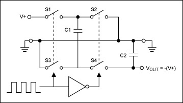
Figure 1: In a traditional charge-pump device, an integrated oscillator opens and closes internal switches, using the flying capacitor, C1, to transfer charge from input and boost voltage across the reservoir capacitor, C2, at the output. (Courtesy of Maxim Integrated)
Used in an archetypical charge pump such as the Intersil ICL7660, this simple approach of driving the switches produces an unregulated output voltage, because the integrated oscillator operates at a fixed frequency for all loads. Consequently, output voltage can vary significantly with load current in the ICL7660 and other simple charge pumps (Figure 2).
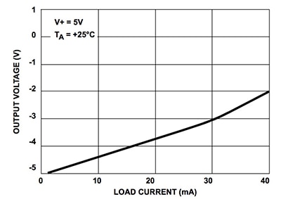
Figure 2: Output voltage can vary significantly with changes in load current in traditional unregulated charge pumps such as the Intersil ICL7660. (Courtesy of Intersil)
A conventional single-output, fixed-frequency device such as the ICL7660 can achieve 90 percent efficiency at low-oscillator frequencies and low-load levels. Operating in low frequency can increase switching losses, however, and at higher frequencies and increasing loads, efficiency can drop significantly. More recent charge-pump devices go further in reaching efficiency levels that in the past were available only from inductor-based switching regulator solutions. For example, the Maxim MAX860 unregulated charge pump IC offers greater than 90 percent efficiency over most of its load-current range.
Regulated output
Designers can provide a regulated supply by using the charge-pump output to drive a simple linear regulator – preferably a low-drop output (LDO) regulator such as the Maxim Integrated MAX8881. Alternatively, designers can find charge pumps that include integrated features for regulated output voltages and multiple power-saving modes. For example, the Maxim Integrated MAX682 delivers a fixed-output voltage across its load-current range (Figure3).
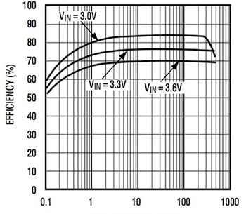
Figure 3: More recent charge-pump devices such as the Maxim Integrated MAX682 offer high efficiency across the greater extent of their load-current range. (Courtesy of Maxim Integrated)
Besides using fixed-frequency switching operation common to charge pump devices, regulated charge pumps use a special skip mode to regulate output voltage. In a skip-mode device such as the Maxim MAX682, an integrated error amplifier disables switching when it detects an output higher than the regulated output voltage (5 V for the MAX682). The device then skips switching cycles until the output voltage drops and the error amplifier reactivates the oscillator. Because skip mode activates only the internal oscillator, devices with skip mode can also exhibit lower quiescent current and lower switching dissipation – particularly important for ambient- and battery-powered wearables and IoT devices.
For many applications, however, the input-voltage level from a battery or energy-harvesting supply varies. In this case, a conventional charge-pump regulator might be driven well outside of its ideal operating envelope, losing efficiency. This condition arises because charge-pump gains are fixed and limited by the number of switching capacitors and on-chip switches. Devices such as the Texas Instruments LM2773 address growing requirements for more flexible charge pumps by integrating control features needed to provide multigain capability (Figure 4). The LM2773 utilizes a regulated charge pump with gains of 2/3x and 1x to operate with an input voltage from 2.5 V to 5.5 V, accommodating single-cell Li-ion batteries. The device produces a selectable regulated 1.8 V or 1.6 V output at loads up to 300 mA.
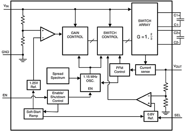
Figure 4: Charge-pump regulators such as the Texas Instruments LM2773 integrate features required for multigain operation, ensuring high efficiency across a wide source-voltage range. (Courtesy of Texas Instruments)
For designs requiring both positive- and negative-voltage supplies, engineers can combine a pair of simple charge-pump devices or, better, turn to multiconverter ICs such as the Linear Technology LTC3265. Built with a pair of charge pumps, the device offers a simple inductor-less solution that combines the ability to work with variable input sources while providing multiple output rails (Figure 5). Each charge pump drives a dedicated LDO regulator able to drive up to 50 mA output current with output voltage levels programmed using external resistor dividers.
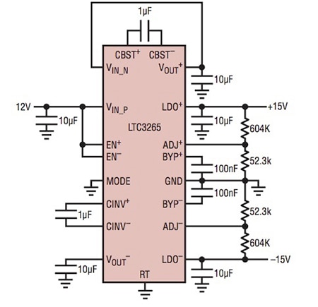
Figure 5: For applications requiring multiple supply rails, the Linear Technology LTC3265 integrates a pair of charge-pump circuits, simplifying design. (Courtesy of Linear Technology)
Ambient- and battery-powered designs often spend much of their operating life in low-power sleep states, waking periodically to sample temperature, heart rate, or some other event with relatively low periodicity. In these applications, the MCU must typically retain previous samples and other state information in internal RAM, which must remain powered to preserve that data even when the MCU enters a low-power mode. Consequently, designers often face the problem of providing power to RAM while shutting down all other power consumers in a regulated supply circuit.
In systems using charge pumps, designers can build a simple solution by using a power management IC to disable the charge pump while continuing to maintain a voltage source to the MCU for RAM retention. For example, designers can insert a Texas Instruments TPS3619 battery backup supervisor IC between a charge pump such as the TI REG710 and an MCU such as the TI MSP430F200 (Figure 6).
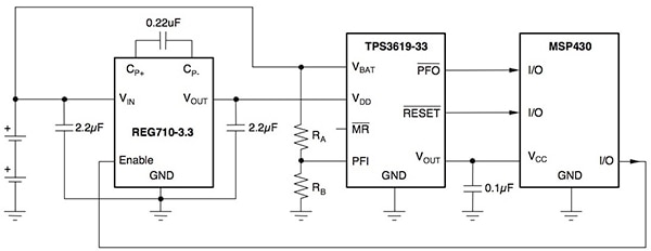
Figure 6: To limit power consumption, designers can shut down a charge-pump regulator such as the TI REG710 using a signal from the MCU. When REG710 output drops below threshold, the TI TSP3619 PMIC can switch the supply source to the battery – providing the MCU with sufficient power to retain RAM state while eliminating power consumption from the REG710 and other circuits. (Courtesy of Texas Instruments)
When the MCU completes its processing, has stored its data, and is ready to slip into a low-power state, it can disable the REG710 charge pump. When the REG710 is disabled, the output voltage decreases until it falls below the TPS3619’s internal trip voltage, VIT. At that point, the TPS3619 will switch VOUT from the output of the REG710 to the VBAT input – so the system consumes minimal power while the MCU continues to receive a supply sufficient for RAM retention.
Summary
Charge-pump devices offer an effective solution for ambient- and battery-powered designs that require voltage regulation capability within the smallest possible footprint. Using small, low-cost ceramic capacitors instead of inductors, these devices now achieve a similar level of efficiency and functional capability once limited to complex inductor-based switching regulators. Unlike earlier charge pumps, today’s charge pump devices are able to operate with varying input sources and multiple outputs, while maintaining regulated output voltage levels across a wide range of load conditions. Using these devices, designers can implement sophisticated voltage supply circuits without compromising the size and functionality requirements of emerging applications in wearables and IoT markets.
For more information about the parts discussed in this article, use the links provided to access product pages on the DigiKey website.
免责声明:各个作者和/或论坛参与者在本网站发表的观点、看法和意见不代表 DigiKey 的观点、看法和意见,也不代表 DigiKey 官方政策。





 中国
中国