How to Simplify Design of a High-Accuracy Polyphase Energy Meter
投稿人:DigiKey 北美编辑
2017-04-18
The Internet of Things (IoT) holds the promise of high-resolution data which can be analyzed for energy monitoring. Where energy metrology was once largely confined to the interface between the power utility and the customer facility, organizations are looking for more detailed information from individual machines and pieces of equipment.
Designing an accurate energy measurement subsystem can be a significant challenge as they require careful attention to the analog signal chain and sophisticated computational capabilities. In the case of three-phase metrology applications, Analog Devices offers a single-chip solution, the ADE9078, which dramatically simplifies implementing solutions for utility meters and power monitoring applications.
This article will dig into the core requirements of a three-phase energy monitoring signal chain, how that chain has evolved, and then introduce the ADE9078 and how to implement it.
The energy monitoring signal chain
Engineers have in the past relied on discrete devices and analog-to-digital converters (ADCs) to build energy meters. The emergence of analog front-end (AFE) ICs allowed engineers to replace complex signal acquisition circuits with a single device that integrated ADCs, amplifiers, and filters into an optimized signal chain. Instead of dealing with the device matching and circuit tuning required by discrete solutions, engineers could rely on the integrated AFE to deliver a properly conditioned signal to an MCU or DSP for calculation of power characteristics.
The integration of MCU or DSP cores into specialized metrology AFEs provided developers with an even more effective solution. Using these devices, engineers could rapidly develop residential energy meters for common single-phase power lines.
For more complex three-phase energy measurement, developers found few effective options aside from once again building custom signal chains using high-performance multi-channel ADCs and amplifiers. Using this approach, however, developers were left to deal with the challenge of not only building tuned signal chains, but also ensuring synchronization of measurements across each phase. Engineers typically opted instead for polyphase meter designs using a separate AFE for each phase as shown in Figure 1.
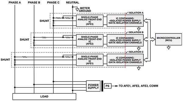
Figure 1: In the past, polyphase energy meter designers needed to combine separate single-phase AFEs and add custom circuitry to measure phase dependent parameters. (Image source: Analog Devices)
Integrated polyphase AFE
Recognizing the designer’s need for a solution to the increasing demand for more efficient solutions, Analog Devices developed the ADE9078 AFE specifically for polyphase energy metering applications. The IC integrates a dedicated metrology engine with a multichannel signal chain driven by seven independent, 24-bit sigma-delta analog-to-digital converters (ADCs) (Figure 2). On the input of each ADC, a programmable gain amplifier (PGA) delivers gains of 1, 2, or 4, while the ADC outputs feed into fourth-order sync filters and decimation filters for anti-aliasing.
The DSP-based metrology engine uses the processed line signals to generate a full complement of parameters required for polyphase measurement applications. In addition, the device supports international standards for both active and reactive energy measurement. Due to its ±25 ppm/°C maximum channel temperature drift, the device delivers the accuracy and stability needed to meet the requirements for utility-grade meters down to Class 0.2.
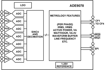
Figure 2: The Analog Devices ADE9078 AFE combines dedicated ADCs with a sophisticated signal chain and metrology engine to provide numerous energy measurements. (Image source: Analog Devices)
Designers need few additional components to build energy meters around the ADE9078. For a typical three-phase four-wire system, designers would use an ADE9078 ADC for each of the three voltage channels (phase A, B and C) with a simple resistor divider used as the voltage sensor on each channel. Similarly, the device’s remaining ADCs would measure the four current channels (phase A, B, C, and neutral) using an appropriate current sensor. At the same time, the ADE9078 eliminates the critical challenge of synchronizing inputs because the ADCs sample their respective signals simultaneously.
Rather than forcing designers to use a power-consuming current shunt as illustrated in Figure 1, the ADE9078 supports more efficient current sensor options including current transformers (CTs) and Rogowski coils. While the device’s built-in compensation features mitigate phase and gain non-linearity found in CTs, its built-in digital integrator enables the use of highly efficient di/dt devices such as Rogowski coils.
In practice, designers need to filter sensor inputs sufficiently to attenuate out-of-band signals (Figure 3). Further, Rogowski coils can generate significant high-frequency noise, requiring at least a second-order anti-aliasing filter. Designers also need to incorporate a similar filter on the voltage inputs to eliminate phase differences between voltage and current measurements.

Figure 3: Although sensor inputs to the Analog Devices ADE9078 AFE require basic RC filters to limit high-frequency signals, the device itself integrates features to compensate for sensor non-linearity. (Image source: Analog Devices)
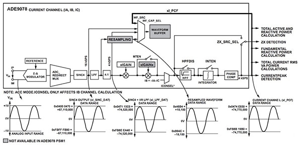
Within the device itself, the ADCs, filters, and metrology combine to create a sophisticated signal chain (Figure 4). At each stage of the chain, associated device registers allow software control of their performance. These registers provide a mechanism for correction of the nonlinearities of CT sensors to achieve very high meter accuracy. Setting the MTEN register, designers can implement midpoint corrections to adjust gain and phase compensation. Additionally, they can adjust the current channel gain, xIGAINx, to correct for gain error due to CT gain non-linearity, or adjust the phase compensation register, xPHCALx, to correct for phase errors.
Figure 4: Engineers can modify the characteristics of the ADE9078 AFE’s signal-processing pipeline simply by changing the register values associated with different pipeline stages. (Image source: Analog Devices)
The ADE9078 provides literally hundreds of registers that provide visibility into and control over nearly every aspect of device operation. Developers read and set device register values through the ADE9078’s SPI-compatible interface. For example, to read the current value of a register, the developer uses a simple protocol where a 16-bit word combines the target register’s address and a flag indicating read access (Figure 5a). The device returns the value of the requested register or registers if burst mode is enabled (Figure 5b).
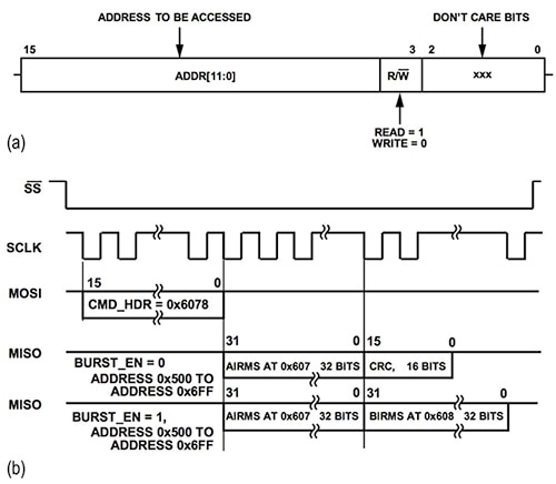
Figure 5: Using a simple command header containing the appropriate register address (A), the ADE9078 uses a simple protocol to read (shown here) or write individual registers (BURST_EN=0) or a series of registers (BURST_EN=1). (Image source: Analog Devices)
Operating modes
The ADE9078 continuously monitors its two power mode pins PM1 and PM0 and enters one of four corresponding power modes depending on the pin levels (Table 1). Typically, designers would operate the device in normal mode (PSM0) which provides full functionality, and use idle mode (PSM3) for a low power reset state.

Table 1. By setting the value of the PM0 and PM1 pins, designers control the operating mode of the ADE9078. (Table source: Analog Devices)
The other two power modes, PSM1 and PSM2, offer tamper measurement and current peak detect, respectively. In current peak detect mode (PSM2), the device uses its integrated low-power comparator to check if the input currents are above a programmable threshold level. In tamper measurement mode (PSM1), the device rapidly measures key parameters including IRMS, VRMS, active power, and reactive power. Since the SPI interface is disabled in this mode, the ADE9078 uses its interrupt pins, IRQ0 and IRQ1, to signal the host processor of the apparent tampering event. In a typical use scenario, the developer would cycle the ADE9078 between normal or idle operating modes, periodically switching to PSM2 to test for tampering.
The extensive integrated functionality of the ADE9078 requires relatively little additional hardware to deploy in a design. Software setup is equally straightforward. Designers minimally only need to configure registers to set gain levels within the signal chain, configure the device for 50 or 60 Hz lines, and enable the digital integrator if a Rogowski coil is used for current sensing. After a 1 is written to the device’s run register, the ADE9078 begins generating results in as little as 40 ms. Typically, designers also need to execute gain calibration to account for device manufacturing variations, and perform phase calibration if CT sensors are used.
Development support
To help developers gain experience with the ADE9078, Analog Devices offers the EVAL-ADE9078EBZ evaluation board and accompanying software. Designers need to add their own CT devices or Rogowski coils for current sensing. In addition, a host processor is required for SPI control and monitoring of the ADE9078. While developers can use their own controller board and processor, Analog Devices recommends using the EVAL-SDP-CB1Z, a controller board based on the company’s Blackfin DSP.
Analog Devices offers a free driver for custom software development that defines mnemonics for all the device’s data and configuration registers, and implements the previously mentioned SPI protocol for reads and writes. For designers that are just beginning to work with the ADE9078, the Windows-based software supplied with the evaluation board is particularly useful in gaining insight into device operation.
The evaluation software provides separate screens for examining registers, interrupts, power quality, and computed energy values. Most of the screens allow the user to explore the device’s internals. On the RMS screen, for example, the user can configure different stages of the signal chain, set register values, and view the effect of those changes on the computed RMS result (Figure 6).
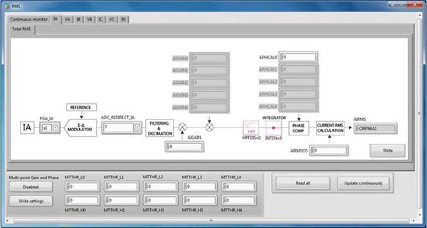
Figure 6: Along with an ADE9078 evaluation board, the Analog Devices EVAL-ADE9078EBZ evaluation kit includes software that lets engineers explore and modify internal device characteristics including the signal chain shown here. (Image source: Analog Devices)
Conclusion
In the past, designers faced significant challenges in building accurate polyphase energy meters. The methods available required designing custom signal-chains or combining single-phase AFEs. Still, those approaches could do little to satisfy the range of requirements associated with high-performance measurement of multiple voltage and current signals.
To help designers answer customer demands for smaller, simpler and more efficient solutions, the Analog Devices ADE9078 combines a sophisticated signal chain with dedicated ADCs in a single device that simplifies design while eliminating traditional obstacles to polyphase energy meter design. Utilizing the ADE9078, designers can rapidly implement sophisticated solutions able to meet the energy metering requirements for performance, accuracy, and reliability.

免责声明:各个作者和/或论坛参与者在本网站发表的观点、看法和意见不代表 DigiKey 的观点、看法和意见,也不代表 DigiKey 官方政策。


