Going Beyond the Datasheet: Understanding LDO Parameters
投稿人:电子产品
2012-10-09
The use of low-dropout regulators, also known as LDOs, is common in many applications because they provide a simple and inexpensive way to regulate an output voltage that must be stepped down from a higher input voltage. What is more, linear LDOs are easy to implement and contribute very low noise as compared to switching regulators.
While LDO specs are straightforward and easy to comprehend, some applications may require a deeper look at key parameters to ensure that the regulator is suitable for the intended application and meets the overall circuit requirements. Unfortunately, datasheets do not provide all the specs under all the possible operating conditions. In such situations, the designer must interpret and extrapolate the available information to determine performance under non-specified conditions.
This capability requires that a designer have a good understanding of LDO specs and features. In addition to the information provided here, I recommend reading “Understanding Low Drop Out (LDO) Regulators” by Michael Day of Texas Instruments,¹ which provides a basic understanding of the dropout performance of a linear LDO regulator. It also shows you how both LDO and system parameters affect an LDO’s dropout performance, as well as its operation. Another suggested article is “Understanding Features and Specs of today’s LDOs” by Kevin Tretter of Microchip Technology.²
Key LDO parameters
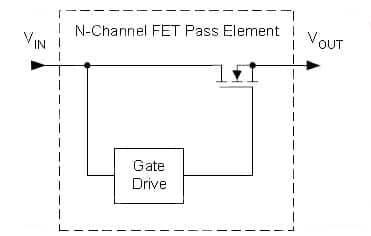
The explanation starts with the basic spec dropout voltage, which is the minimum voltage required across the regulator to maintain regulation. For instance, a 3.3 V LDO regulator with 1 V dropout will require a minimum input of 4.3 V. To understand the meaning of voltage drop across the LDO, let’s look at a fundamental LDO architecture with a pass element. As shown in Figure 1, the pass element can be an N- or P-channel FET, which provides the voltage drop as a function of FET’s on-resistance, RDS(on).

Figure 1: LDO’s pass element can be an N- or P-channel FET (Courtesy of TI).
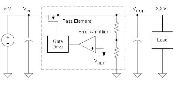
In essence, the LDO behaves like a variable resistor whose resistance value is controlled by the error amplifier shown in Figure 2. Normally, if the input was a constant source, the LDO could simply be replaced by a resistor. But, in reality, the input source is never constant, so feedback is necessary to alter the LDO’s effective resistance to maintain the desired regulated output voltage. Depending on the input voltage or load current, the error amplifier drives the pass element’s gate to maintain a constant output voltage.

Figure 2: Fundamental LDO block diagram (Courtesy of TI).
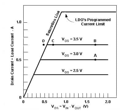
However, there are restrictions and boundary conditions based on the FET’s V-I curve, beyond which the LDO will not perform as desired. As depicted in Figure 3, the x-axis is the FET’s drain to source voltage VDSM, which is VIN – VOUT for an LDO, while the y-axis represents the pass FET transistor’s drain current in amperes (A). Using this curve, an engineer can determine the dropout voltage at any operating current. In fact, the pass element’s gate-to-source voltage must be controlled with changes in input voltage or load current to maintain the desired output regulation, as shown in Figure 3.

Figure 3: Operating region of LDO’s N-channel pass element (Courtesy of TI).
The dropout is normally specified by the manufacturer. For instance, take TI’s TPS79330. The maximum dropout voltage specified for this LDO is 200 mV for a 3.0-V output and 200-mA current. The minimum RDS(on) for this LDO is given as RDS(on) = 200 mV/200 mA = 1 Ω. With minimum input voltage of 3.15 V for this regulator, the effective dropout voltage required for this part must be less than 150 mV at 200-mA load current.
The dropout voltage at any other current is calculated by multiplying the minimum RDS(on) by the actual load current. So if the load current is 170 mA, the dropout voltage at this current would be VDO = 1 Ω x 170 mA = 170 mV.
This is still not low enough to ensure regulation. The designer must find an LDO with a lower dropout voltage at 170 mA to meet desired requirements. TI offers a large array of LDOs to select from. Besides TI, some other LDO suppliers include Analog Devices, Fairchild Semiconductor, Linear Technology, ON Semiconductor, Microchip Technology, and Maxim Integrated, to name a few.
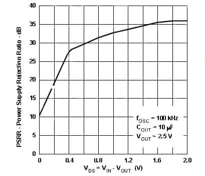
Similarly, some other parameters influencing an LDO’s performance include power supply rejection ratio (PSRR) and output noise. PSRR affects the LDO's ability to prevent output voltage fluctuations caused by variations in input voltage. It is usually expressed in decibels at a specific frequency. A typical plot of LDO’s input to output voltage differential VDS for VOUT of 2.5 V is shown in Figure 4. It shows that below 0.4-V VDS, LDO’s PSRR starts falling rapidly. For good output performance, the PSRR must be high.

Figure 4: Typical plot of an LDO’s power supply rejection ratio (PSRR) versus input to output voltage differential (Courtesy of TI).
An LDO's internal voltage reference is a potential source of noise. This noise is fed directly into the error amplifier shown previously in Figure 2. The noise on the output of this amplifier modulates the FET’s gate voltage, further increasing LDO’s output noise. As per the discussion in reference 1, the designer must determine tradeoff between high PSRR and low noise performance. TI’s TPS799xx family offers high PSRR with low noise performance.
As we have seen, designers must be aware of various specifications of the LDO beyond those prominently placed on a datasheet; he or she also must know how these specifications affect the overall system design. This article has discussed key parameters and presented sample parts. For more information on these products, use the links provided to access product information pages on the DigiKey website.
References
- “Understanding Low Drop Out (LDO) Regulators”, Michael Day, Texas Instruments
- “Understanding features and specs of today’s LDOs”, Kevin Tretter, Microchip Technology, Electronic Products, March 2010.
免责声明:各个作者和/或论坛参与者在本网站发表的观点、看法和意见不代表 DigiKey 的观点、看法和意见,也不代表 DigiKey 官方政策。


 中国
中国