Building Wireless Backhaul for Wired Networks
投稿人:DigiKey 欧洲编辑
2013-09-26
This article looks at the challenges of building wireless backhaul links to support wired networks, using a range of different technologies, from microwave for rural areas to WiMax for in-filling urban networks.
Wired networks sometimes need a bit of wireless. This is particularly true in telecom networks, where wireless might be a cost effective way to replace a short leased line, or used to provide links that are just too expensive to wire up. Backhaul from wireless base stations is often provided by wireless links in rural areas, as the cost of installing new fixed lines to the base station can be prohibitively expensive. New technologies such as WiMax have emerged to make wireless links for backhaul more cost effective even in urban areas.
Microwave links have been commonly used for many years as an integral part of a wired network. The wireless link bridges gaps in the network that come from geography or politics as simple wire replacements. These are in the regulated wireless spectrum to prevent interference and provide reliable connections, but at a higher cost in both licensing and equipment, as they are limited to point-to-point (PTP) links.
These links have evolved from a PTP link to include point-to-multipoint (PTMP) to distribute data and voice to several separate points, but often uses a number of point-to-point links fanning out from one central location. They are also making use of technologies such as OFDM in the unlicensed bands for PTMP connections.
Licensed microwave links typically operate in the 6 GHz, 11 GHz, 18 GHz, and 23 GHz spectrums. Additionally, there is a 60 GHz unlicensed band that is of interest to component makers, although this is aiming at short-range point-to-point wire replacement rather than the longer distance telecom applications.
However, 24 GHz is an unlicensed frequency that can be used for microwave communication for point-to-point wireless backhaul, and can be used for either line of sight (LOS) or non line of sight (NLOS) applications. This offers some key advantages for a wireless Ethernet bridge, as it is identical to the 23 GHz band and can be used for shorter range wireless links, usually under 2 miles. As it is rarely used, there is little to no wireless interference, and manufacturers that make 24 GHz microwave communication radios for the 23 GHz licensed microwave links can use the same carrier grade microwave radio platform adjusted to operate at 24 GHz. A microwave backhaul link system can do up to 366 Mbps full duplex using 256QAM at 56 MHz wide channels.
Most 24 GHz microwave communication links can be installed as a 100 Mbps full duplex wireless backhaul and can be software upgraded up to 360 Mbps full duplex (720 Mbps aggregate throughput).
For a point-to-point backhaul to work in an NLOS design, several requirements need to be met – a proper power budget, fade mitigation, adaptive link characteristics, and proper demodulation in regards to dispersion. Because of obstructions in a NLOS situation, there tends to be a large amount of multipath. Obstructions like trees add to multipath and add attenuation to the overall path loss of the microwave link. Trees can be tricky because they are not constant due to movement caused by wind, foliage changes during various seasons, moisture content of the foliage, and more. Constant obstructions like buildings or hills are easier to model and predict.
The other frequently used unlicensed frequency bands are the more common 900 MHz, 2.4 GHz, 5.3 GHz, 5.4 GHz, and 5.8 GHz spectrums, and the choice of band determines the system design.
Using DSSS in the 2.4G Hz band provides an ideal low-cost point-to-multipoint solution where a clear line of sight exists between the base station and subscribers. This is ideal for community broadband in rural areas where a point of presence is then extended to a number of subscribers around the village, town, or area. The antennas are usually two types, omnidirectional and sector type, typically 60 – 120 degree beam width.
Alternatively, 5.8 GHz OFDM is used for higher data-rate applications and where there is no clear line of sight between the base station and subscribers. This can be used as the backbone connection to multiple wireless ‘hot-spots’ around the town or area to deliver community-wide broadband in urban and rural areas, where a point of presence is then extended to a number of subscribers, typically businesses around the town or area. The antennas are usually sector type, typically 120 degree beam width, and these links can deliver both IP Ethernet data and E1 voice.

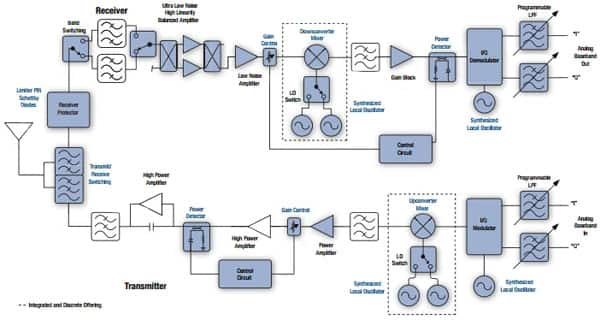
Figure 1: A simplified infrastructure transceiver.
Skyworks’ Low Noise Amplifiers (LNA) meet the demanding ultra-low noise figure and high linearity needs of receiver designs. Using a pseudomorphic high-electron mobility transistor (pHEMT) design with silicon germanium (SiGe) and Heterojunction Bipolar Transistor (HBT) processes, these amplifiers have the flexibility to achieve the necessary gain and linearity specifications. The LNA family of two-stage cascaded LNAs includes discrete packaged transistors and high-linearity, low-noise driver amplifiers operating over the 0.7 – 1.2 GHz, 1.7 – 2.4 GHz, and 2.3 – 2.7 GHz frequency bands. The devices integrate the inter stage matching network on die to reduce the number of external components required. These support unconditional stability up to 18 GHz and >18 dB return loss while maintaining 0.7 dB noise figure. The same layout is used for all devices, simplifying design for all available frequency bands.
The discrete packaged transistors have the flexibility to be used in numerous low noise applications. The SKY65050-372LF and SKY65052-377LF are 200 µm pHEMTs designed for low power applications operating with a bias as low as 2 V, 5 mA. The SKY65052-372LF and SKY65051-377LF are 400 µm pHEMTs designed for high-linearity, low-noise applications.
Skyworks’ low-noise driver amplifiers are ideal choices for mid-stage amplification in receiver designs. The devices feature flat gain response, ≤ 2 dB noise figure, and high linearity performance. Devices require minimal external components to simplify the design and lower overall cost.
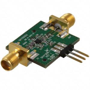
The Skyworks SKY65053-377LF (Figure 2) is a high-performance, N-channel low-noise pHEMT transistor in a 2 x 2 mm, four-pin Quad Flat No-Lead (QFN) package.

Figure 2: The SKY65053-377LF transistor on an evaluation board.
The 400-micron periphery of the SKY65053-377LF makes the device extremely versatile with a wide, useable frequency bandwidth, low NF, and high linearity. The frequency range extends from roughly 200 MHz through 6 GHz. This low-noise pHEMT is easily adapted for use in multiple applications by tailoring its external impedance-matching circuits. Supply current is controlled with one external bias resistor, which allows the IDS to be selected from 20 mA to 100 mA. This enables the SKY65053-377LF to be used for many different applications such as those requiring a very-low NF (when biased at a low IDS) and high linearity (when biased at a high IDS).
WiMax
WiMax may have waned in popularity over the last few years, but it has had a significant impact as a cost-effective point-to-point backhaul link technology. The point-to-multipoint capability can reduce the cabling needed to link multiple base stations in an urban environment, saving costs in cable installation and still making use of standard equipment.
For a piece of equipment to be WiMax certified by the WiMax Forum, it must comply with the 802.16 IEEE standards and be completely interoperable with other manufacturers’ equipment. The FCC in the US has opened up the 3.65 GHz band for licensed operations, and many mobile carriers provide WiMax using their privately owned spectrum (typically in the 2 GHz range).
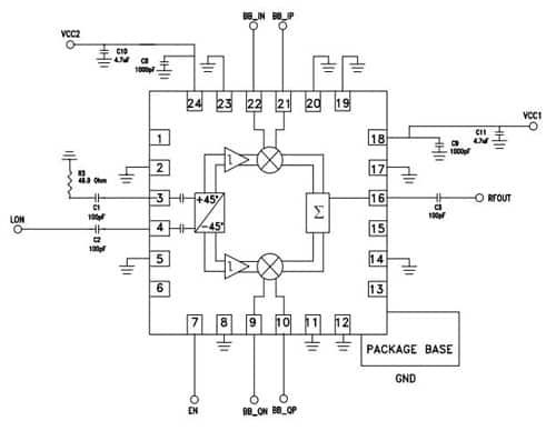
The HMC1097LP4E from Hittite Microwave (Figure 3) is a low-noise, high-linearity direct-quadrature modulator RFIC, which is ideal for digital modulation applications from 0.1 to 6.0 GHz including WiMAX/4G, broadband wireless access, and ISM circuits.

Figure 3: The HMC1097LP4E quadrature modulator from Hittite Microwave.
Housed in a compact 4 x 4 mm (LP4) SMT QFN package, the RFIC requires minimal external components and provides a low-cost alternative to more complicated double upconversion architectures. The RF output port is single-ended and matched to 50 Ohms with no external components. The local oscillator (LO) requires -6 to +6 dBm and can be driven in either differential or single-ended mode. This device is optimized for a +5 V supply, and offers improved carrier feedthrough and sideband suppression characteristics. It offers an easy-to-use, complete direct-conversion solution in a highly compact 4 x 4 mm plastic package, thereby reducing cost, area, and power consumption.
The LO interface consists of a LO quadrature phase splitter that generates two carrier signals in quadrature, followed by LO-limiting amplifiers used to drive the I and Q mixers with saturated signal levels. Therefore, the LO path is immune to large variations in the LO input signal level and the modulator performance does not vary much with LO input power.
The LO input impedance is set by the LO quadrature phase splitter. The LO port can be driven differentially with 100 Ω differential input impedance or single-ended through LON input with 50 Ω input impedance, while the unused LOP input should be terminated to GND through 50 Ω. The LO port requires -6 to +6 dBm input power in either differential or single-ended mode and does not require DC blocking capacitors.
For the I/Q modulator, the differential baseband inputs (QP, QN, IP, and IN) present a high impedance. The DC common-mode voltage at the baseband inputs sets the currents in the I and Q double-balanced mixers. The nominal baseband input DC common-mode voltage used in the characterization of the HMC1097LP4E is 0.45 V, which should be externally applied.
The baseband input DC common-mode voltage can be varied between 0.4 V and 0.5 V to optimize overall modulator performance. It is not recommended to leave the baseband inputs floating, which generates excessive current flow that may cause damage to the IC. The baseband inputs should be pulled down to GND in shutdown mode. The nominal baseband input AC voltage used in the characterization of the HMC1097LP4E is 1.3 VPP differential. The baseband input AC voltage can be varied to optimize overall modulator performance. Hittite recommends driving the baseband inputs differentially to reduce even-order distortion products, and also using reconstruction filters at the baseband inputs to avoid aliasing.
After upconversion, the outputs of the I and Q mixers are summed together differentially and converted to a single-ended RF output. The single-ended RF output port is internally matched to 50 Ohms and does not require any external matching components. Only a standard DC-blocking capacitor is required at this interface and it requires a single supply voltage of +5 V to operate.
The EN pin can be used to disable the bandgap reference circuit that supplies the different blocks. Disabling the bias circuit will also disable the reference currents to the LO limiting amplifiers, I and Q mixers, and the output stage. If the EN pin is connected to ground or left floating, the part operates normally. If the EN pin is connected to the +5 V VCC, the LO limiting amplifiers, I and Q mixers, and the output stage are disabled and the LO leakage is also reduced. The LO signal itself is suppressed approximately by 57.1 dB at 2.1 GHz when the EN pin is connected to the +5 V VCC. The enable and disable settling times are approximately 400 ns.
The carrier feedthrough is related to the DC offsets at the differential baseband inputs of the modulator. If exactly the same DC common-mode voltage is applied to each of the baseband inputs, and there were no DC offsets at the differential baseband inputs, the LO leakage at the RF output would be perfectly suppressed. By adding small DC offset voltages at the differential baseband inputs, the carrier feedthrough can be optimized for a specific frequency band and LO power level. The carrier feed-through cannot be calibrated by the DC common mode level at the I and Q baseband inputs. DC offsets at the differential I and Q baseband inputs should be iteratively adjusted until a minimum carrier feed-through level is obtained. Externally available offset voltage steps and the modulator’s noise floor limit the minimum achievable calibrated carrier feed-through level. The typical offset voltages for optimization are less than 15 mV.
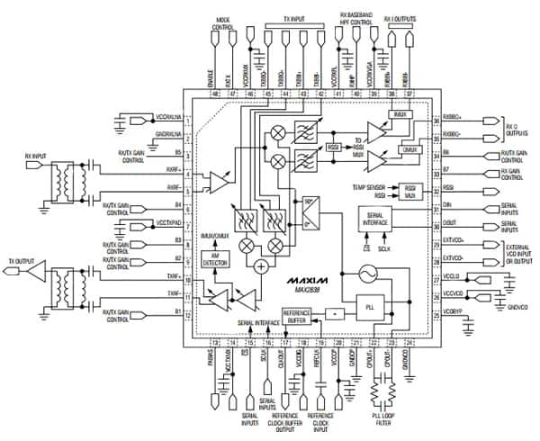
The MAX2838 from Maxim Integrated (Figure 4) is a direct-conversion, zero-IF, RF transceiver designed specifically for 3.3 GHz to 3.9 GHz wireless broadband systems including NLOS links. The MAX2838 completely integrates all circuitry required to implement the RF transceiver function, providing RF-to-baseband receive path, baseband-to-RF transmit path, VCO, frequency synthesizer, and baseband/control interface. The device includes a fast-settling sigma-delta RF synthesizer with smaller than 29 Hz frequency steps.

The MAX2838 supports 2Tx, 2Rx MIMO applications with a master device providing coherent LO to the slave device. The transceiver IC also integrates circuits for on-chip DC-offset cancellation, I/Q error, and carrier leakage detection circuits. Only an RF bandpass filter (BPF), TCXO, RF switch, PA, and a small number of passive components are needed to form a complete wireless broadband RF radio solution.
The MAX2838 completely eliminates the need for an external SAW filter by implementing on-chip monolithic filters for both the receiver and transmitter. The baseband filters along with the Rx and Tx signal paths are optimized to meet the stringent noise figure and linearity specifications. The device supports up to 2048-FFT OFDM and implements programmable channel filters for 1.5 MHz to 28 MHz RF channel bandwidths, making it suitable for WiMax link applications. The transceiver requires only 2 µs Tx-Rx switching time and the IC is available in a small, 48-pin, thin QFN package measuring only 6 mm x 6 mm x 0.8 mm.
To boost a WiMax link further, NXP Semiconductors’ 75 W LDMOS power transistor supports applications at frequencies from 2500 MHz to 2700 MHz, including building WiMax links. The channel bandwidth is 1.2288 MHz at a frequency of 2500 MHz and 2700 MHz, a supply voltage of 28 V, and an IDq of 600 mA. With an average output power of 9 W and power gain of 17 dB, the transistor has easy power control, integrated ESD protection, and the ruggedness needed for an outdoor application.
Conclusion
Using a wireless link as a cable replacement is increasingly popular in many areas, both rural and urban. Urban areas are using WiMax to link base stations together more efficiently, while rural areas use the microwave links to provide vital data services to areas that cannot be easily reached with cabling. Building wireless transceivers to bridge the ‘difficult’ miles, via line-of-sight or non-line-of-sight systems, brings high bandwidth services to isolated communities.

免责声明:各个作者和/或论坛参与者在本网站发表的观点、看法和意见不代表 DigiKey 的观点、看法和意见,也不代表 DigiKey 官方政策。


