Buck-Boost Converters Enable Flexible Energy-Harvesting Designs
投稿人:电子产品
2013-06-12
For energy-harvesting applications with highly variable energy sources, engineers can find themselves dealing with output voltages that can range higher or lower than levels needed to charge a typical energy storage cell. In the past, designers dealt with this situation by following a boost stage with a separate buck converter to ensure proper voltage output levels. Single-chip buck-boost converters provide a convenient alternative by generating an output voltage that can be less than, equal to, or greater than the input voltage. To meet the challenges of harvesting power from highly variable energy sources, engineers now can simplify their designs using buck-boost ICs from Analog Devices, Linear Technology, Maxim Integrated, and Texas Instruments, among others.
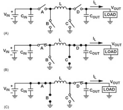
Buck/boost converters contain four switches, two capacitors and an inductor (Figure 1A). In operation, high-efficiency buck-boost devices operate only two of the four switches, reducing losses and improving efficiency.
When VIN is greater than VOUT, switch C is open and switch D is closed and switches A and B operate as in a standard buck regulator (Figure 1B), switching the output voltage according to the pulse-width modulation (PWM) frequency to create a lower output level. When VIN is less than VOUT, switch B is open and switch A is closed, leaving switches C and D to operate as in a boost regulator (Figure 1C), charging and discharging the inductor to boost the output above VIN. When VIN is near VOUT, the device operates in buck-boost mode where buck and boost operations occur as needed during a switching cycle.
Device manufacturers take special care to reduce losses, optimize efficiency, and eliminate instability due to mode switching. Fundamentally, the goal for design of these devices is to provide effective voltage regulation with minimal current ripple in the inductor to guarantee good transient performance. As a result, circuit designers can incorporate these devices with minimal additional circuitry to achieve well-regulated output despite widely varying input voltages.
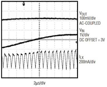
For example, the Maxim Integrated MAX8625 IC uses Maxim’s proprietary H-bridge topology to deliver a virtually glitch-free transition through all operating modes (Figure 2). The device combines four internal MOSFETs (two switches and two synchronous rectifiers) with internal compensation to minimize external components.
Indeed, devices in this class require relatively few external components to deliver regulated output despite wide-ranging VIN. For example, the Linear Technology LTC3129 integrates switches and associated circuitry, requiring only a few external passive components along with a pair of BAS70-05 Schottky diodes for operation with many energy-harvesting input sources (Figure. 3).
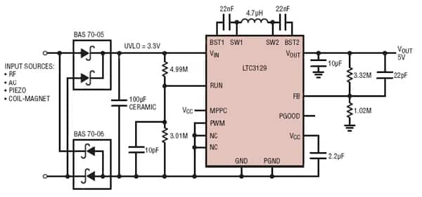
The LTC3129 uses a proprietary switch control algorithm to maintain output voltage regulation with glitch-free transitions between buck and boost operating modes. The LTC3129 features both wide VIN (1.92 to 15 V) and VOUT (1.4 to 15.75 V), while providing a 200 mA output current in buck mode. The device requires only 10 nA in shutdown mode and runs with a quiescent current of only 1.3 μA. The LTC3129 also provides a maximum power point (MPP) control function that allows engineers to program the input voltage for operating energy-harvesting power sources at their ideal load. Engineers can also use the device's RUN comparator to turn the converter on and off at specific VIN threshold values with hysteresis.
Other available buck-boost converters from Linear offer designers a range of options for dealing with highly variable power sources. The LTC3534 features more limited ranges for VIN (2.4 to 7 V) and VOUT (1.8 to 7 V) but can achieve relative high output current levels with its integrated switch network. Along with 25 μA quiescent current, this device features a fixed 1 MHz operating frequency, sub-1 μA shutdown, short-circuit protection, programmable soft-start, current limit and thermal overload protection.
For wider input voltage ranges, the Linear LTC3780, and LTC3789 feature VIN of 4 to 36 V and 4 to 38 V, respectively, using external MOSFET switches for higher current capabilities. For high efficiency operation at light loads, both devices can be configured to operate in forced continuous conduction mode or in a skip-cycle mode. Here, the devices hold switches in their current state for a number of cycles until specific operating conditions are reached.
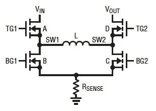
For example, in pulse-skipping mode in the boost region, the LTC3789 holds off the output high-side synchronous switch (switch D in Figure 4) whenever reverse current through switch A is detected. At very light loads, the current comparator may remain tripped for several cycles and force switch C to stay off, skipping the same number of cycles. In buck operation, the device does not allow inductor current to reverse. Here, the current comparator may remain untripped for several cycles at very light loads, holding switch A off for the same number of cycles while synchronous switch B also remains off for the same number of skipped cycles. In buck-boost operation, the controller alternates between the boost and buck region in one clock cycle as in continuous operation.
The Analog Devices ADP2503 and ADP2504 ICs operate with input voltages between 2.3 and 5.5 V and support various fixed-output options. An adjustable model allows engineers to program the output voltage using an external resistor divider. For power savings at light loads, the devices can enter a power-save mode that reduces the switching frequency. In applications such as wireless sensor nodes, where the use of variable frequency in power-save mode could result in interference, the devices can be set to force fixed-frequency PWM operation under all load conditions.
The Texas Instruments TPS63030 (VIN 3.6 to 5.5 V) and TPS63036 (VIN 1.8 to 5.5 V) devices similarly offer an optional power-save mode for operation at light loads. In this mode, these converters stop operating, allowing the output voltage to drop at a rate depending on the load and the value of the output capacitance. When output voltage falls below a threshold value, these devices resume operation for one or more cycles. Engineers can disable power-save mode to force these devices to operate at their fixed frequency.
Conclusions
For energy-harvesting applications that face widely varying input voltages, integrated buck-boost converters offer a suitable alternative to techniques using separate boost and buck circuit stages. Using available buck-boost converter ICs, engineers can design highly flexible energy-harvesting applications able to accommodate diverse input voltage conditions. For more information on the parts mentioned in this article, use the links provided to access product pages on the DigiKey website.
免责声明:各个作者和/或论坛参与者在本网站发表的观点、看法和意见不代表 DigiKey 的观点、看法和意见,也不代表 DigiKey 官方政策。





 中国
中国