Basics of Direct Digital Synthesis
投稿人:电子产品
2013-10-03
Direct digital synthesis (DDS) is a technique for generating waveforms of arbitrary frequency, with an output that can be easily slewed or tuned to another frequency or phase without discontinuities, phase shifts, or other artifacts. It is used for tuning and frequency control in wireless systems that must sweep across a wide range of frequencies or support many discrete channels in applications such as wireless communications systems, frequency-agile radar, and time-domain reflectometry (TDR). DDS is an attractive alternative to other synthesis techniques such as phase-lock loops (PLLs) and FPGA plus DAC, as it offers superior performance with a smaller footprint, less power, and lower cost in many applications.
Principles of DDS
DDS is a technique for generating waveforms that does not use any traditional "oscillator" approaches. Instead, it synthesizes, or creates, the amplitude-versus-time points of a waveform using digital memory and buffers, in conjunction with a digital/analog converter output stage. Further, the DDS output does not have to be a sine wave; it can be a triangle, square, or any other wave shape. Note that even though we think of it as a frequency synthesizer, many of the concepts of DDS center on "phase." This is not a problem because phase and frequency are intimately related; frequency is the time rate of change (derivative) of phase, and conversely, phase is the time integral of frequency.
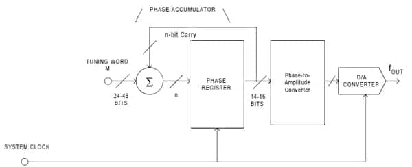
There are three primary functional blocks in a DDS system (Figure 1), an accumulator (consisting of a phase register and summing junction), a phase-to-digital converter (a memory block also called a phase-to-amplitude converter), and a digital/analog converter (D/A converter). It requires a reference frequency input (usually from a precision or crystal clock) that is divided down by a scaling factor, which itself is established by a binary tuning word and is an input to the accumulator.

The phase accumulator generates a number corresponding to the phase angle of the desired output waveform, while the phase-to-digital converter generates the instantaneous digital fraction of the output amplitude which occurs at that specific phase angle. Finally, the D/A converter provides an analog output based on the value of the phase-angle data (Figure 2). For a sine-wave output, the phase-to-digital converter is just a lookup table of sine-wave values, but other tables can be used for other waveforms.

You can think of the DDS operation as an incremented counter stepping through the entries in the lookup table of the phase-to-digital converter. To change frequency, just change the rate at which you increment the counter. How can you do that, given that you have a fixed-frequency reference clock fc at the heart of the DDS? You do this by using a fixed-frequency clock and a numerically controlled oscillator (NCO). The phase accumulator counts by N to generate a frequency Fout related to fc by the simple equation:

where M is the resolution of the tuning word (24 to 48 bits, depending on DDS design), and N is the number of pulses of fc, matching the smallest incremental phase change of the phase accumulator's output word. Therefore, the tuning word defines the output frequency as a fraction of the reference clock frequency.
To change phase or frequency, the tuning word is changed and the output slews directly to the new frequency/phase, without any bumps, discontinuities, or other undesired distortion. As a result, DDS is well suited for fast, agile frequency hopping, whether in a cell phone or a military radar jammer.
Although this is a digital technique, the performance of the D/A converter is a major factor in purity of output and overall performance. It may be a separate IC from the all-digital elements, or a single, larger IC, depending on required performance, the design and process capabilities of the vendor, cost, and test issues. A high-resolution, high-speed, high-performance D/A converter is needed for almost all DDS applications.
Performance parameters
Since the D/A converter is key, its specifications often limit the DDS performance. Fortunately, there are many standalone D/A converters or one-chip DDS plus D/A converter components with very good performance, so the technique is quite useful.
The D/A converter output is a series of distinct amplitude points, not a smooth sine wave (or other waveform). For the most common situation, a sine wave, the D/A converter output is a string of pulses with a sine-like time envelope. In the frequency domain, this corresponds to a fundamental frequency and its aliases (images), with the usual sin x/x envelope (Figure 3).
A low-pass filter is used to attenuate these images and enhance the purity of the fundamental (baseband) sine output. Since the first image's amplitude is just 3 dB below the fundamental's amplitude, the design of this filter and how it suppresses images is critical. Following the Nyquist criteria for sampling, the maximum output frequency is one-half the D/A converter's output update rate.

Key DDS specifications include:
- Spurious-free dynamic range (SFDR) is the strength ratio of the fundamental signal to the strongest spurious signal in the output. It is the ratio of the RMS value of the maximum signal component, the carrier or fundamental, at the output of DAC to the RMS value of the next-largest spurious output (spur) component; it is usually measured in dBc (dB with respect to the carrier) and typically has values between 60 and 100 dBc.
- Phase noise and jitter (various sources) are two perspectives on the same error sources in many ways, either in the frequency domain (phase) or time domain (jitter). Sources include jitter in the reference clock, which is outside the actual DDS circuitry but still affects final performance.
- The performance of the D/A converter itself. Independent of the other DDS elements, there are the customary issues of linearity, quantization errors, and other well-known dynamic sources of converter errors.
- Though not intuitively obvious, any truncation of the phase-register output can result in code-dependent errors. While binary-coded words do not cause such truncation errors, non-binary-coded words and consequent phase-noise truncation errors will produce spurs in the spectrum.
- Bandwidth affects the rate at which the DDS output can slew to new frequencies without distortion.
Vendors offer both components which can be used to build a DDS function, as well as single-IC solutions. In addition, they offer evaluation kits which simplify test and assessment, while eliminating problems associated with layout and PC board design.
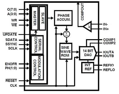
Intersil's ISL5314 is a complete DDS function in a 48-lead package (Figure 4). It includes a 14-bit D/A converter and can provide output with sample update rates to 125 Msamples/s. The 16-bit NCO (rounded down to 14 bits for the DAC) is controlled by the sum of a 48-bit center-frequency word, a 48-bit offset-frequency word, and a 40-bit serially loaded tuning word. For fast tuning, the NCO is loaded via a parallel interface, while a serial interface is used for overall IC control to reduce pin count and package size.

The AD9952 from Analog Devices also includes a 14-bit D/A converter, but can update at up to 400 Msamples/s for sine waves up to 200 MHz (Figure 5). Phase noise is better than ̵120 dBc/Hz at 1 kHz, with SFDR of at least 80 dB. The low-power 1.8 V IC (5 V I/O for digital interface compatibility) uses serial format for both overall control, as well as loading of its 32-bit tuning word, to minimize package size.

For complete performance evaluation, the AD9958/PCB from Analog Devices supports the AD9958, a dual-channel, 500 Msample/s, 10-bit DDS IC. The board (Figure 6) includes PC evaluation software for control and measurement of the AD9958, a USB interface for connection to the PC used for setup and evaluation, and graphic user interface (GUI) software with frequency-sweep capability for board control and data analysis.

Summary
Direct digital synthesis (DDS) is a technique for generating and changing waveforms of arbitrary frequency without discontinuities, phase shifts, or other artifacts. It is used for tuning and frequency control in systems which must sweep across a wide range of frequencies or support many discrete channels. DDS is an attractive alternative to other synthesis techniques such as phase-lock loops (PLLs) and FPGA plus DAC, in terms of performance, power, and cost.
免责声明:各个作者和/或论坛参与者在本网站发表的观点、看法和意见不代表 DigiKey 的观点、看法和意见,也不代表 DigiKey 官方政策。


