Minimizing Jitter/Phase Noise in Clock-Distribution Topology is Critical to Wireless Performance
投稿人:电子产品
2016-04-29
The days of RF circuits being all-analog designs are long gone; today’s RF designs rely on heavily digital functions such as their PLL-based synthesizer (tuner) and A/D and D/A converters. Increasingly, these synthesizers and converters are being used directly at higher frequencies, wider bandwidths, and for direct conversion designs or software-defined radio (SDR).
The consequence is that the clock, as seen by the ICs it supports, must be more "pure" than ever. Why is this? The reason is that any deviation in the clock, usually characterized as timing jitter or phase noise, will degrade achievable component performance. Clock jitter/phase noise means that the effective number of bits (ENOB) of an A/D converter will be lower than its nominal resolution, and other parameters such as SFDR, SNR, distortion, and intermodulation products will also be adversely affected. The allowed numbers are astonishingly tight: In many of the newest designs, allowable maximum clock jitter at the load IC is on the order of a few fsec.
[Note that timing jitter and phase noise are two equally legitimate perspectives on the same imperfection, with jitter being a time-domain number while phase noise is a frequency-domain number. Depending on the error analysis, designers need to use one or the other, but neither factor is inherently a superior way of looking at clock issues.]
For these reasons, designs place a great deal of emphasis on producing and delivering a high-accuracy clock for the various ICs which require them. It is not just a matter of generating the clock, as a quality crystal in conjunction with various high-end clock-oscillator/generator ICs can provide the clock needed. The real challenge is ensuring the clock signals reach the loads intact, without noise or jitter.
The situation is complicated by two factors: the same clock signal may be needed at various locations of the PC board; and different clock signals (often derived from the same crystal, using a multi-output clock-generator IC) are needed as well. This places an intra-clock skew limit on the clock signals. The designer's challenge is to decide, in a given application, on an overall clock-distribution topology which not only produces the primary clock(s), but also ensures that the clock signal(s) reach their loads with acceptably low jitter and skew.
Basic one clock, several loads
The simplest situation is where a master clock must go to several loads, such as multiple A/D and D/A converters for a multi-channel system. As an example, let’s use a basic software-defined radio (SDR) which has two A/D converters (for I and Q receiver channels) and a complementary pair of D/A converters for the transit channel.
One approach often used successfully is to locate the system clock generator (and its crystal) such that the electrical distance and thus propagation delay to each converter is identical, (Figure 1); most clock-generator ICs can directly drive multiple loads. However, care must be used to equalize the electrical distance to each converter to minimize inter-channel skew, and each track must maintain a nominal 50 Ω impedance (in most applications) to minimize transmission-line reflections. Further, the path of the each clock must be routed carefully with respect to nearby high-speed digital lines which may add noise to the clock signals due to RFI/EMI. Adding all these up, it’s a lot of demands and constraints placed on the clock signals.
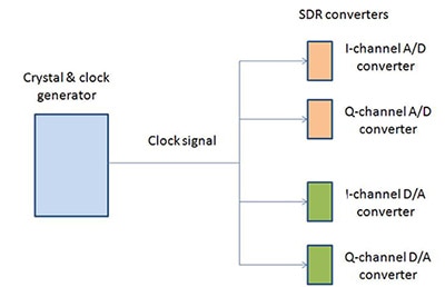
Figure 1: Basic clock distribution to a software-defined radio begins with low-jitter clocks to the I- and Q-channel A/D and D/A pairs of the receiver and transmitter, respectively.
A step up is to use a fan-out buffer as close to the converter cluster as possible, and start building a clock tree. These ICs, which are a useful building block of many clock trees, provide signal buffering and multiple low-skew copies of the input signal. The clock fan out from a single input reduces loading on the preceding driver and provides an efficient clock distribution network. In this example, they can be used to place the apparent clock source much closer to the converters (Figure 2). Among these buffers are some specifically designed to re-clock the original clock signal and so reduce jitter (sometimes called "clock cleaners" as a slang term).
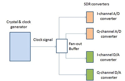
Figure 2: A localized fan-out buffer can maintain clock integrity across the multiple loads, but at a cost in component and power.
Even with a fan-out buffer, the per-clock propagation delays may be outside the allowable specification. For this, a variation of the fan-out buffer called a zero-delay buffer is used (Figure 3). These are PLL-based devices that regenerate the input clock signal (with fan out, to drive multiple loads if needed), and also allow the delay through the device to be adjusted, via an external feedback path. By doing so, they allow precise control of the timing of the clock signals to the loads and can compensate for local skew variations.
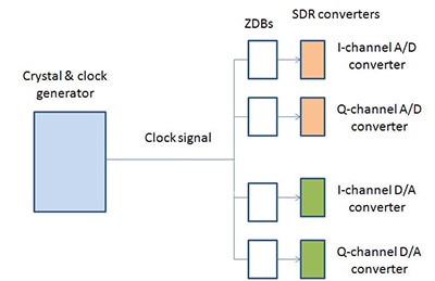
Figure 3: Zero-delay buffers can not only reduce jitter, but also allow fine-tuning of propagation delay and thus skew across multiple channels.
For example, the IDT2308B from Integrated Device Technology (Figure 4) is a high-speed phase-lock loop (PLL) clock multiplier which achieves zero delay by aligning the phase between the incoming clock and the output clock, and operates from 10 to 133 MHz. It has two banks of four outputs each that are controlled via two select addresses for flexibility in configuration.
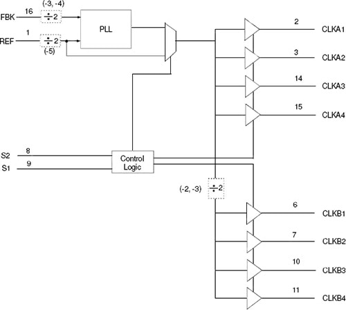
Figure 4: The IDT2308B from Integrated Device Technology is representation of a zero-delay buffer; due to its external PLL feedback loop, it can be used to effectively reduce delay to zero or add in precise delays to equalize lags.
Other loads, other sources
In general, it’s a better use of PC board space, power dissipation, and BOM cost to have fewer crystals in a circuit. In the SDR example, the system FPGA needs a high-speed, ultralow-jitter clock, but at a frequency which may be very different than the A/D and D/A converters (and with different electrical characteristics, as well). Rather than begin an entirely new clock chain with a separate crystal and clock-generator IC, a universal clock generator can be used to “tap off” the primary clock and generate the clock frequency for the FPGA (Figure 5). The clocks will be electrically buffered and independent of each other, yet the parts count is kept low.
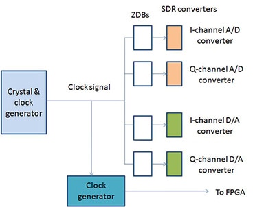
Figure 5: Programmable clock generators can use an existing clock at an unrelated frequency as their source, thus eliminating the need for another crystal and clock oscillator.
For example, the Silicon Laboratories Si5338 generates any frequency on any of its four differential outputs or eight single-ended outputs from 160 kHz to 350 MHz, and select frequencies to 710 MHz (Figure 6). It supports a wide variety of output formats, including LVPECL, LVDS, HCSL, LVCMOS, HSTL, SSTL, and CML, and outputs have rms phase jitter which is under 1 psec.
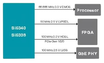
Figure 6: Any-frequency, any-output clock generators such as the Si5338 (or Si5340) from Silicon Laboratories can provide the multiple, different frequency/format clocks needed in many communications systems, thus simplifying the clock tree while minimizing jitter at the clock loads.
For each new clock needed, the clock tree grows a new clock-generator that can make use of existing clocks. Note that these do not have to be additional ICs, as some clock-generator vendors offer ICs with four or more independent clock outputs driven by a single-input clock. Again, it’s important to check the jitter specifications of these clocks, to make sure they are compatible with the needs of the loads they serve.
Modeling, simulations are critical
The first step when assessing the timing is to work out basic margins and error buildup of possible topologies based on specific vendor clock-related generators and buffers. Vendors offer various basic tools to simplify this process and assess some of the topology trade-offs. They also offer expert online tools where you to enter your clock requirements and see possible clock-tree topologies.
However, these vendor tools cannot assess clock performance in the actual physical PCB layout. As clock frequencies increase, the layout considerations are also increasing. Designers must verify the timing, noise, and other clock-signal parameters for their layout using appropriate signal-integrity tools and even EM simulation as clocks move into the hundreds of MHz and even low GHz range. Vendors provide specific guidelines for layout of clock signals and representative reference designs which will minimize unexpected or unpleasant surprises; these should be carefully studied and factored into the PCB layout design-constraint list.
Summary
In a large, complicated circuit such as an SDR or cellular base station, it’s fairly common to have a dozen or more unrelated clock frequencies to serve the needs of converters, FPGAs, specialty ASICs, I/O, and more. By looking at the options early on, and then simulating them, designers can find the various "sweet spots" balancing the many desired attributes and priorities of performance, power, price, and layout flexibility for their clock-tree distribution topology. The up-front analysis may also need to be verified using modeling and simulation which takes other physical-layout factors into account.
For more information about the parts discussed in this article, use the links provided to access product pages on the DigiKey website.
Further Reading:
- AN-815, "Understanding Jitter Units."
- AN-827, "Application Relevance of Clock Jitter."
免责声明:各个作者和/或论坛参与者在本网站发表的观点、看法和意见不代表 DigiKey 的观点、看法和意见,也不代表 DigiKey 官方政策。


