Designing Compensator Networks to Improve Switching Regulator Frequency Response
投稿人:电子产品
2015-10-07
A DC-to-DC switching voltage converter’s (or “switching regulator”) control loop can be characterized by its frequency response. The frequency response influences the switching regulator’s reaction time to transient changes, precision, and stability and in turn how well it maintains a set voltage output under variations in the input voltage, load, and duty cycle.
Engineers can improve the frequency response of a switching regulator by adding compensator networks. The objective is to tune the frequency response such that the switching regulator’s crossover frequency is positioned optimally (providing high bandwidth) yet the unit has enough phase- and gain-margin for good dynamic response, line and load regulation, and stability. If the job is done well, the end result is a switching regulator that’s stable over a wide frequency range yet is not overcompensated so that its dynamic response is poor.
This article describes the basics of compensator networks for switching regulators and explains how the types of network influence the power supply’s frequency response and ultimate performance.
Countering instability
All too frequently a design engineer can find his or her initial circuit layout for a switching regulator proves unstable. Instability can cause noise from the magnetic components or ceramic capacitors, jittering in the switching waveforms, oscillation of output voltage, overheating of power Field Effect Transistors (FETs) and other undesirable side effects. Figure 1 shows typical output waveforms from an unstable step-down (“buck”) switching regulator.
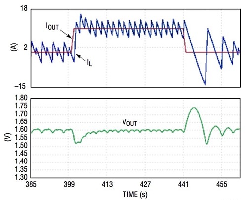
Figure 1: Current and voltage output from an unstable switching regulator. (Courtesy of Linear Technology)
Although there are many causes of instability––for example, noise generated by the PCB––one common culprit is under-compensation of the power supply’s control loop. To address this problem the engineer must add a compensation network. Properly implemented, the output of a compensation network (A(s)) together with the feedback voltage (VFB) divider will tune control-loop characteristics to ensure DC (zero frequency) gain is high, crossover frequency (or bandwidth) (fc) is high, and good phase- and gain-margins result in a switching regulator with good dynamic response, line- and load-regulation, and stability.
The performance of the switching regulator’s control loop is quantified by the loop bandwidth and the loop-stability margin. The bandwidth is defined by the crossover frequency, at which the loop gain equals one (0 dB). Higher bandwidth aids fast transient response at the expense of loop-stability margin and control loop sensitivity to switching noise. The loop-stability margin is typically quantified by the phase margin and gain margin. The phase margin is defined as the difference between the overall phase delay and -180° at the crossover frequency, while the gain margin is the gain at a phase lag of 180°.
Assuming the gain plot crosses 0 dB only once (which for voltage regulators with a low-pass filter at the output stage is virtually always the case) the system will be stable if the phase lag at the crossover frequency is less than 180°. Experienced engineers aim to achieve a phase margin greater than 45° (and less than 315°). Typically, a phase margin of 45° is a good compromise between transient response and damping. For boost or buck-switching regulators the gain margin should be above 10 dB.
Types of compensation network
Switching regulators employ closed feedback loops to regulate the output voltage. Figure 2 shows a voltage-mode control scheme typical of buck controllers. The compensation network forms a feedback circuit for the error amplifier. Since the introduction of the switching regulator engineers have developed three kinds of commonly employed compensation networks (named after the number of zeroes and poles that they introduce into the control loop), Types I, II, and III.
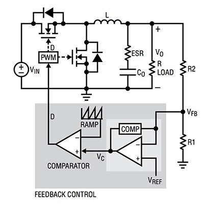
Figure 2: Buck-switching regulator control loop with compensation network added to error amplifier. (Courtesy of Linear Technology)
Type 1 compensation maximizes the DC gain of the circuit, which in turn minimizes DC regulation error. The compensation is achieved by adding a capacitor (Cth) to the output of the error amplifier. The addition of the capacitor creates an integration term within A(s) with an infinitely high DC gain. The downside of adding the capacitor is that it introduces a -90 degrees phase lag which, combined with other feedback-loop phase lags, can push the circuit close to instability.
Manufacturers helpfully provide an error amplifier output pin on their modules (such as the “ITH” pin on Linear Technology’s LTC3851, a synchronous, buck-switching regulator controller with a maximum switching frequency of 810 kHz). A quick test to check if the control loop is the source of instability in a power supply can be performed by connecting a large capacitance (for example 0.1 µF) to this pin. If lack of compensation is the cause of the circuit’s instability, the capacitor will typically reduce the power supply’s bandwidth to a low-frequency inducing stability. If the capacitor has no effect, the engineer is advised to look elsewhere for sources of instability.
A resistor (Rth) can be added in series with the original capacitor to improve stability. The effect of the resistor is to add in a “zero” (Sthz) contributing a +90 phase lead. The trick is to select the correct value of resistor such that the phase lead is introduced before the crossover frequency, thus increasing the phase significantly at that frequency, improving the voltage loop’s phase margin and stability. Figure 3 shows a small signal model of such a compensation network and a Bode plot of its frequency response (superimposed on the effect of the capacitor alone (dashed blue line)). Note how the additional zero boosts the phase margin at the crossover frequency.
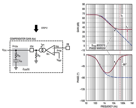
Figure 3: Small-signal model showing error amplifier and resistor/capacitor compensation network and associated Bode plot. (Courtesy of Linear Technology)
Unfortunately, the resistor does more than just contribute a phase lead; it also boosts the gain at high frequencies. This side effect increases the likelihood that noise generated by the power components at the switching regulator’s operational frequency (which is typically high) will affect the output.
The solution is to add a second capacitor (Cthp), of a value much lower than Cth, as close to the ITH pin of the power module as possible, connecting the pin to ground. The introduction of this second capacitor introduces a high-frequency “pole” into the Bode plot that should ideally be located between the crossover frequency and the switching frequency (fs). The effect of the pole is to reduce gain around the switching frequency. (The component might also decrease the phase at the crossover frequency so its value must be chosen carefully to trade off noise immunity against phase margin.) Such a two (II)-pole, one-zero compensation network is known as Type II.
Figure 4 shows a Type II compensation network recommended for use with an Intersil ISL85415 buck-switching regulator. The device runs at a switching frequency of 500 kHz, requires an input of 3 to 36 V and supplies an output of 0.6 to 34 V at up to 500 mA.
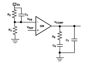
Figure 4: Type II compensation network for an Intersil buck converter.
Figure 5 shows the Bode plots for the buck converter using the compensation network shown in Figure 4. With this compensation network, the switching converter has a 75 kHz bandwidth with a 61° phase margin and 6 dB gain margin.
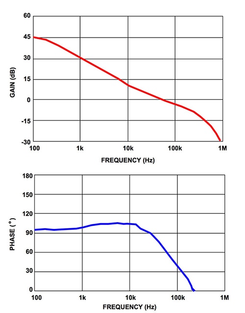
Figure 5: Bode plots for the Intersil buck converter using compensation network shown in Figure 4.
While a Type II compensation network can work well, further refinement of the power supply’s frequency response can be achieved by implementing a more complex compensation network which shapes the profile of the gain with respect to frequency in a similar fashion to the Type II network but takes things slightly further. This network features three (III) poles and two (or three) zeroes and is known as Type III.
As with the Type II network described above, the low-frequency pole provides high-DC gain to minimize DC-regulation error and the first high-frequency pole is placed to cancel the zero generated by the output filter capacitor’s equivalent series resistance (ESR) zero (fESR). As with the Type II network, the second high-frequency pole is placed after the crossover frequency to attenuate switching noise in the feedback loop without compromising phase margin significantly. The inductor and capacitor cause other zeroes in the power stage.
Type III compensation is complicated and time consuming, since it requires finding the optimum combination of six R/C values. Power module manufacturer Intersil offers some guidelines for an initial calculation of these values in reference [3]. Figure 6 shows a Type III compensation network. The circuit leads to the frequency response for the converter shown in Figure 7. It is important that the compensation network gain does not exceed the open loop gain of the error amplifier.
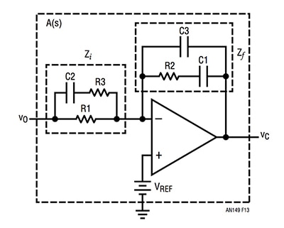
Figure 6: Type III compensation network. (Courtesy of Linear Technology)
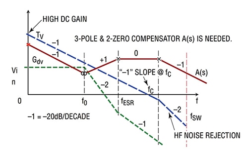
Figure 7: Switching regulator frequency response (blue) using the compensation network shown in Figure 6 with the frequency response A(s) (red). (Courtesy of Linear Technology)
Analytical software
An initial calculation of Type III compensation network values should be considered a guide only and it is recommended that the actual gain and phase plots are generated through the use of a commercially available analytical software package with the capability to plot. Once the gain and phase plots are generated the component values might need to be altered slightly for a better response.
All the major power module manufacturers supply software packages to make compensation network design a relatively simple process. For example, Linear Technology provides its LTpowerCAD, which the company describes as “a complete power supply design tool program that can significantly ease the tasks of power supply design.” Similarly, Intersil offers its PowerNavigator software (primarily for digital power supplies), Fairchild Semiconductor supplies Power Supply WebDesigner and Texas Instruments’ (TI) Power Stage Designer Tool “helps design the power stage of the most commonly used switch mode power supplies.”
Another option that can make life easier for the engineer is to select a chip that features internal compensation. The downside is a loss of flexibility because the designer is stuck with the chip supplier’s compensation scheme, which may not be ideal for his or her application, but the upside is simpler design, fewer external components, and reduced bill-of-material (BOM).
An example of a chip with internal compensation is TI’s LM46000 buck regulator. The chip is able to drive up to 500 mA of load current from an input voltage range of 3.5 to 60 V for a 1 to 28 V output. The LM46000 has an adjustable switching frequency from 200 kHz to 2.2 MHz.
Seek assistance
Designing a switching regulator based on a power module from a semiconductor manufacturer can appear to be straightforward. All the major suppliers provide application circuits for their products that ensure a power supply will operate under a given set of conditions. However, an end product can present a unique set of operating conditions not covered by the application information. Such operating conditions can expose instability in the initial design and demand additional circuitry in the form of a compensation network.
The details of compensation network design are not trivial and require a reasonable understanding of control theory including analysis of poles and zeroes in the S-plane. With inexperience it can be all too easy to overcompensate leading to a design with restricted bandwidth and poor transient response. Such designs require excessive output capacitance to improve the transient response adding to the bill of material (BOM) and power supply size.
Inexperienced engineers are advised to access the online resources of power-module suppliers such as Linear Technology, Fairchild Semiconductor, Intersil, and TI for guidance. In addition, these manufacturers all offer software packages to ease the complexity of loop-compensation network design.
For more information about the parts discussed in this article, use the links provided to access product pages on the DigiKey website.
References:
- Modeling and Loop Compensation Design of Switching Mode Power Supplies,” Henry J. Zhang, Application Note 149, Linear Technology, January 2015.
- “Practical Feedback Loop Design Considerations for Switched Mode Power Supplies,” Hangseok Choi, Ph. D, Fairchild Semiconductor, 2011.
- “Designing Stable Compensation Networks for Single Phase Voltage Mode Buck Regulators,” Doug Mattingly, Technical Brief TB417.1, Intersil, December 2003.
- “Control Loop Design,” Lloyd Dixon, Texas Instruments, 2001.
免责声明:各个作者和/或论坛参与者在本网站发表的观点、看法和意见不代表 DigiKey 的观点、看法和意见,也不代表 DigiKey 官方政策。
