8-bit MCUs That Can Operate Under 1.8 V
投稿人:电子产品
2013-07-24
Sleep modes and idle modes in general-purpose microcontrollers have allowed embedded processors to reduce real-time energy consumption and tackle many battery- and low-powered designs. However, as embedded systems become increasingly complex, it takes additional logic to implement a denser, more sophisticated micro core as well as the higher-end peripherals we expect to see today. As a result, even in standby modes, static power draw can be an issue when trying to reduce energy, especially if long sleep times are required.
One factor in reducing energy and extending run-time is operating voltage. While many 5 V systems are still around and supported, the majority of designs today have migrated to the 3.3, 2.5, and 1.8 V arenas. With voltage being directly proportional to power draw, you can see that a static 5 V system will burn almost three times the power of a 1.8 V system. This is even more the case with switching circuits, since power draw is also proportional to switching frequency.
This article examines 8-bit microcontrollers with simpler architectures and lower-than- average voltage cores that can operate under 1.8 V. While these levels may not work with most external peripherals, it does allow lower power, long-term sleep/hibernation modes that can extend battery life to its limits. It also allows a micro to stay alive longer as batteries approach a fully discharged state. All parts, datasheets, tutorials, and development resources mentioned here are available on the DigiKey website.
The architecture debate
Well-designed cores with peripherals specifically created to use less energy can make a big difference in your design. Are you using a general-purpose micro or have you selected one of the low-power-architected devices? There are some cleverly designed micros from 8- to 32-bits, featuring low-energy modes that are quite impressive.
A good debate can be made for both sides of the bus-width argument. On one side, you can say that bigger 32-bit architecture can process faster. Because of this, the wider architecture does not need to remain awake as long and can ultimately save power (even though it is keeping alive a much wider architecture).
On the other hand, a narrower architecture, like an 8-bit machine, can do all the processing required, albeit taking longer, but will sleep with much less power in static state. Registers, memory, pointers, and more, are all narrower in bus width, meaning less static power draw.
This debate gets interesting when you look at some of the low-voltage 8-bit parts that have rich peripherals and features, mixed-signal functionality, and a lot of I/O. A perfect example comes from ROHM with its Lapis series of ML610 low-power processors.
While relatively meager in some respects, these parts with low-voltage cores have an admirable mix of peripherals and flavors, including some typical configurations such as the 120-pin TQFP ML610Q422P with 32K of flash and 2K of RAM and the 144-pin LQFP ML610Q431 with 64 K of flash and 3K of RAM.
The ROHM series is made up of high-performance CMOS 8-bit microcontrollers built-in with Lapis Semiconductor's original RISC 8-bit CPU "U8 Core." The CPU core is capable of efficient instruction execution with one instruction per one cycle clock operation. The “610” family of products is popular for battery-driven, handheld-type applications in a variety of fields.
Note that these parts do not run with high-megahertz clocks. They save power by running the processors at low frequencies (typically 4 MHz) and using a RISC core executing most instructions in 244 µs. Like other low-energy processors, these processors can also operate using the real-time clock’s 32.768 kHz. While slower (30.5 µs per instruction cycle), they can draw correspondingly less current.
The key is these cores have a guaranteed operating range down to 1.1 V. This allows some clever adaptive power supply design techniques, especially if your processor is going to be shutting down and sleeping for a long time.
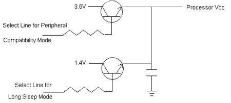
For example, when interfacing externally via a serial port or standardized 3.3 V peripheral, an I/O line can set VCC to 3.3 V using an I/O driven transistor or biased D/A level (Figure 1). Peripheral chips can be powered up and down the same way if they do not have low-power modes. When no external activity is needed, VCC can be set to 1.8 or even 1.1 V. This dynamic approach to power supply voltages can be applied to any core that can operate reliably below the 1.8 V threshold.

In addition to basic UART, I²C, and SPI connectivity, a variety of higher-end options are available such as LCD interfaces, external bus interfacing with GPIO, and other unusual peripherals like a melody generator. Of particular interest for low-power distributed sensor applications is that these parts contain two 16-bit A/D converters and 24-bit D/A converters.
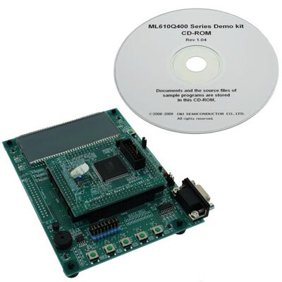
The ROHM ML610QX demo board uses plug-in daughterboards to house the individual ML610 family members (Figure 2). The motherboard contains an LCD, serial port, pushbuttons, and an enunciator to help test basic coding and designs. The UEASE W/ COMPILER is also available for compiler and emulator/debug support.

Another interesting part comes from STMicroelectronics; their STM8L101G2U6A operates down to 1.62 V. The part is one of ST’s EnergyLite Series, with up to 68 I/O and up to 64 K of flash and 8K of RAM. The 8-bit core is based around a CISC architecture with an internal 16 MHz R/C oscillator and draws 300 nA in Halt mode and 800 nA in Active-Halt mode (retention of all internals).
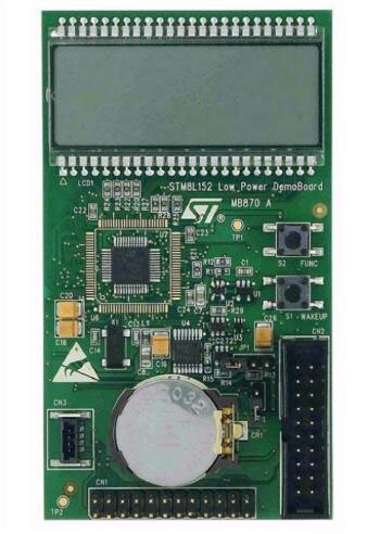
These are not blazingly fast, ultra-dense parts, but they are not intended to break any speed records. Peripherals supported are similar to those of other processors aiming at low-power designs, with basic functionality like SPI, IIC, and UART. These parts target cost-sensitive, low-power applications and can use ST’s STM8L15LPBOARD for application test and development, supporting the company’s STM8L EnergyLite processors (Figure 3). A schematic¹ of the development board is also available and these processors are supported by the Segger Flasher Series Production Tools.

It should be noted here that while 1.62 V is not significantly different to 1.8 V as far as power savings goes, it does mean that the processor can run longer as a battery or super-cap is discharging, especially running at low frequencies.
Down to 0.5 V
One of the many advanced 8051 cores that stand out among the crowd comes from Cypress, with their CY8C32xx family Programmable Systems on a Chip 3 (PSoC3). These are a family of system-level chips that combine analog, digital, peripheral, memory, and a CPU on a single chip.
Like other highly refined 8051 cores, PSoC3 builds on the familiar architecture with modern single-cycle speeds (50 MHz in this case) and high-end peripherals (such as LCD, DMA, USB 2.0, and Touch Sense), and goes beyond any legacy parts. One block in particular stands out in this context.
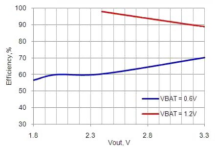
While rated to run from a minimum 1.71 V, these parts can actually run from voltages as low as 0.5 V (yes, you read that correctly). An internal high-efficiency boost regulator steps-up low input voltages (from 0.5 to 1.8 V) to 5 V to power the system on a chip and its peripherals (Figure 4).

Mixed-signal functionality is also supported. These parts have two 12-bit A/D converters. A D/A with 8-bit resolution may be limiting, but there is plenty of I/O (up to 62) and peripheral buses — including IIC, SPI, UART, LIN, and USB — from which to hang external D/A’s. Another nice feature is its on-chip EEPROM (up to 2K x 8), which can be written to under software control for nonvolatile parameters.
A typical middle-of-the-road example would be the 100-pin LQFP CY8C3245 with 32K of flash, 1K of RAM, and 1K of EEPROM. This part features a lot of I/O (62) and can implement an external bus interface to expand memory range or add parallel peripherals.
In conclusion
Low-power and energy-sensitive designs can reduce real-time power draw by lowering their core voltages. Several manufacturers realize this and meet demand by offering parts that can still run when others have exhausted their batteries.
While 8-bit parts can benefit from this approach, engineers should not lose sight of the fact that there are also 16- and 32-bit low-voltage cores offering their own power-saving techniques. So keep an open mind as you select MCUs for your next project.
For more information on the parts discussed in this article, use the links provided to access product pages on the DigiKey website.
References
- Schematic of STMicroelectronics STM8L development board
免责声明:各个作者和/或论坛参与者在本网站发表的观点、看法和意见不代表 DigiKey 的观点、看法和意见,也不代表 DigiKey 官方政策。


