Use Log Amps to Enhance Sensitivity and Performance in Wide-Dynamic-Range RF and Optical Links
投稿人:DigiKey 北美编辑
2017-08-02
Received signals in RF and some optical data links may span a wide dynamic range of 100 dB or more. Their signal strength often varies continuously and uncontrollably due to changing channel conditions, antenna position, and other factors. The challenge for receive channel designers is to scale this wide-ranging signal so as to maximize front-end sensitivity with low-level signals while not overloading the system on the higher magnitude ones. The result of scaling is improved signal/noise ratio, enhanced channel sensitivity, and better SNR performance.
A conventional linear amplifier, regardless of its other capabilities, cannot handle this wide range of signals. What is needed instead is an amplifier that continually measures the wide-ranging signal level of the input in real time so the system can use that strength indication to control the channel’s gain parameters.
The solution comes in the form of a specialized, all analog logarithmic amplifier (log amp). This device produces an output voltage that is proportional to the logarithm (log) of the input signal’s amplitude. A log amp can handle signals with a dynamic range from 50 up to 100 dB or more, and at frequencies into the hundreds of megahertz (MHz) and even gigahertz (GHz).
Since the output is the log of the input value, that output can span many decades of input range amplitude. Recall that 60 dB corresponds to a 1000:1 voltage ratio or three orders of magnitude, while 100 dB corresponds to a 100,000:1 voltage ratio or five orders of magnitude.
This feature will describe the applications and characteristics of log amps, pin point key parameters, advise on how to select a log amp, and provide examples of log amps and their typical application.
Applications include receive, transmit paths
The log amp can be used to solve multiple, diverse RF and fiber-optic channel issues. Let’s discuss three: cellular base stations, radar and sonar, and power amplifiers.
1: Cellular base station receivers must accommodate signals from phones which are located at varying distances, in wide-ranging and ever-changing conditions due to motion and orientation, interference, shielding, and other factors which are beyond the control of the cell phone user. Similarly, longer range radio receivers serving both mundane terrestrial services as well as exotic spacecraft must accept signals with constantly changing signal strength due to propagation conditions and other uncontrollable issues with the signal path environment.
To dynamically adjust receiver front-end gain, the log amp is used to provide a received signal strength indicator (RSSI) similar to an “envelope detector” (Figure 1). This indicator signal, in turn, is critical to maintaining optimum control of the gain of the signal chain despite the widely varying conditions. Doing so allows the subsequent demodulation circuit to operate on a tightly bounded, well-defined signal amplitude. This maximizes demodulator performance in terms of accuracy, linearity, and bit error rate (BER) (for digital signals).
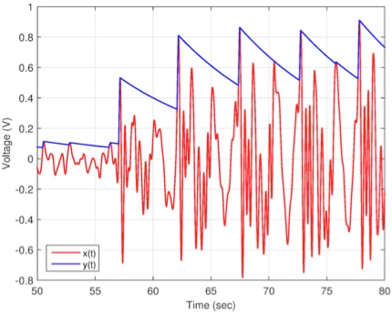
Figure 1: The logarithmic amplifier captures the “envelope” or outline magnitude of a signal, but on a scale that is logarithmically related to the signal value. (Image source: Missouri University of Science and Technology)
In many ways, an RSSI indicator based on a log amp is a greatly enhanced, higher performance, wider range version of the automatic gain control (AGC) function which has been in use from the earliest days of broadcasting and receiving (Figure 2). In the AGC, a basic “envelope detector” develops a voltage corresponding to the intensity of the modulated received signal’s overall power at any instant, and then uses that voltage to control the gain of the front-end amplifier.
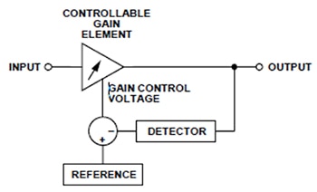
Figure 2: The traditional automatic gain control (AGC) function uses a detector, often comprising a diode and capacitor, to assess the signal magnitude and then close the loop to a voltage-controlled amplifier to minimize variations in the signal envelope’s magnitude. However, it lacks the dynamic range that a log amp offers. (Image source: Analog Devices, Inc.)
However, widely varying RF signals are not just an issue in communications links.
2: In radar and sonar systems, log amps also play an important role. Here, the received signal is an echo reflection, the strength of which is a function of distance to target, target size and type, atmospheric or water conditions, and many other factors (Figure 3). As a result, the signal strength is unknown, varies widely, is distorted compared to the original pulse, and is beyond control of the system.
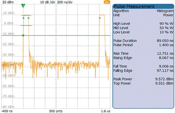
Figure 3: Radar and sonar signal returns are known for having wide, fast-changing dynamic range, due to the largely unknown and uncontrollable nature of the target and its echo, as well as the medium’s variability (air or water). Here, the dynamic range exceeds 50 dB. (Image source: Rohde & Schwarz)
3: In power amplifiers (PAs), log amps are increasingly needed even for the fully internal, tightly controlled path running just a few centimeters between a transmitter’s PA and its antenna in a cell phone or similar portable devices. The reason is that these devices must now work with internal antennas, which are unavoidably “detuned” from their nominal, designed impedance match by the user’s body or environment. Yet for satisfactory performance, the voltage standing wave ratio (VSWR) between PA and antenna must be kept as close as possible to 1:1, with 2:1 as the maximum allowed value in most cases.
The solution is to measure the incident and reflected RF signals between the PA and antenna, which can then be used to determine VSWR and its changes in real time that result from user motion, body interference, and many other factors. This works because the ratio of incident (transmitted power) to reflected power can be used to calculate the VSWR. Once VSWR is known, the wireless device can dynamically adjust the matching circuit between the PA and antenna to keep VSWR below 2:1, assuming this capability has been designed into the device.
However, measuring the forward and reflected signal to calculate VSWR is not trivial. It requires a directional coupler to isolate and then sample the incident and reflected power between the PA and the mismatched load (Figure 4). Two log amps are needed: one for incident waveform and one for reflected waveform, each of which can vary over tens of dB. The ratio between incident power and reflected power is the key number needed to calculate VSWR.
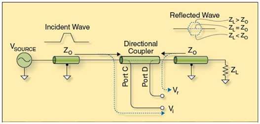
Figure 4: Dual log amps are now used to characterize PA-to-antenna VSWR and thus support dynamic adjustments to keep VSWR close to unity and so maximize power delivered to the antenna, based on simultaneous measurements at Port C (incident wave) and Port D (reflected wave). (Image source: Analog Devices, Inc.)
Clearly, this is getting complicated in terms of components, bill of materials, and circuit subtleties. Fortunately, log amps also allow for a “trick” which greatly simplifies the calculation of the incident/reflected power ratio and subsequent matching circuit adjustment.
Use Log amps to simplify VSWR matching circuit adjustment
Since the two measured signals are logarithms, the subtraction of one from the other is equivalent to division (ratio) of their pre-logarithm numbers. By using a pair of log amplifiers, and then a simple analog subtraction function using an op amp, the critical ratio of the incident/reflection power can be determined in real time without the need for numeric processing. In contrast, doing this division numerically would be impractical, as it would require two high-resolution, high-speed analog-to-digital converters (ADCs) followed by fast numeric processing.
In general, the widest application of log amps is to measure the strength of a received signal and, rather than detect or demodulate its content, use this signal strength reading to control channel gain or adjust other system parameters. However, the dynamic VSWR optimization technique described here is increasingly being applied by designers of portable devices as it allows the devices to operate in multiple bands, with one or more antennas.
Log amp principles and implementation
The basic relationship between input VIN/output VOUT of a log amp is simple:
VOUT = VY log(VIN/VX)
Where VY and VX are scaling factors. However, putting theory into practice is not so simple. There are several topologies in use, all of them using the logarithmic voltage/current relationship of the PN diode as their fundamental building block, (Figure 5).
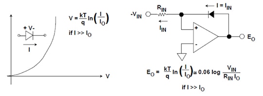
Figure 5: The principle that makes analog log amps possible is simple and basic, making use of the inherent current/voltage relationship in a PN diode. However, creating a wide-ranging, accurate log amplifier is very difficult. (Image source: Analog Devices, Inc.)
Designers of log amps – initially using hybrid circuits and modules, now almost always using ICs – have leveraged this physical relationship with innovative configurations which use multiple stages for wide range while minimizing errors at either end of the scale, as well as during the main part of the range (Figure 6). A single log amp IC can now provide accurate performance over a range of 50 dB, 100 dB, or more, depending on the device selected and frequency of operation.
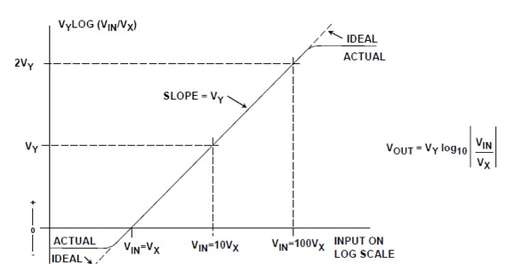
Figure 6: The transfer function of an ideal log amp is linear if the input (horizontal) scale is linear and the output (vertical) scale is logarithmic. (Source: Analog Devices, Inc.)
They have also worked out schemes to ensure minimal error due to temperature coefficient, even though diode parameters are very dependent on temperature. Further, by adding some offsets and absolute value front-end circuitry with the log function, they have developed configurations which work around the fact the logarithm of zero and negative numbers is not defined, yet zero and negative signals are an unavoidable occurrence in the signal chain.
Choosing a log amp
Some of the parameters used to define the performance of log amps differ from those used to assess linear amplifiers since a log amp is, by definition, highly nonlinear. The transfer function of a log amp shows an idealized device that uses the absolute value of the input rather than the actual value, to get around the “negative” input problem (Figure 7).
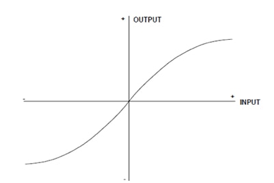
Figure 7: The transfer function of an actual log amp for most applications must also go through zero and into the negative input range (although there are log amps for unique applications which do not need to include this extra consideration). (Image source: Analog Devices, Inc.)
The top level specifications of primary interest are:
- Dynamic range: indicates over how many dB the log amp operation is meaningful and close to ideal; typically, this is 40 to 100 dB.
- Log linearity or log conformance, which is the closeness of the linear/logarithmic transfer function to the ideal equation. This specification can be expressed in different ways, but the most common is maximum deviation from a “perfect” logarithmic function, such as ±0.5 dB over a defined amplitude and frequency range. For most log amps, the vendors provide multiple curves that show the log linearity conformance over the entire range, and under multiple conditions (Figure 8).
- Noise: the noise generated within the amplifier defines the lower boundary of useful signal performance. The wide dynamic range of the log amp is useless if signals at the lower end are overwhelmed by internal noise.
- Frequency response and bandwidth, which can begin at DC in some designs, or at relatively high frequency in others; the upper range can extend to hundreds of MHz and even GHz.
- Slope of the transfer characteristic, expressed as V/dB or mA/dB depending on whether this is a voltage or current output device.
- Intercept point is the input level at which the output voltage or current is zero.
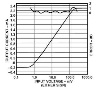
Figure 8: The basic accuracy graph for a log amp shows the deviation from “perfect” in dB along the entire dynamic range specified; here, it is about ±1 dB from 1 mV to 100 mV. (Image source: Analog Devices, Inc.)
Many different log amps are available, each with specifications tailored to a target class of applications. Radar generally needs the widest dynamic range, wireless links require higher frequency capability, and antenna matching optimization requires increased accuracy.
For example, the AD8309 from Analog Devices is a 5 MHz to 500 MHz log amplifier with 100 dB of dynamic range, suitable for signals ranging in amplitude from –78 dBm to +22 dBm (into 50 Ω). It achieves this wide range via a series of cascaded internal stages, the complexity of which is hidden from the user (Figure 9).
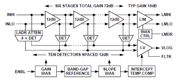
Figure 9: The internal structure of a wide-range, accurate log amp such as the AD8309 requires multiple cascaded substages along with attenuation and detection circuitry, plus error correction and offset functions. Fortunately, this complexity is not seen by the user. (Image source: Analog Devices, Inc.)
The AD8309 features 20 mV/dB slope transfer function, –95 dBm intercept, and ±0.4 dB RSSI linearity up to 200 MHz. It is well suited for very wide range intermediate frequency (IF) and RF power measurement, as well as RSSI indication and control. It can also be used for basic radar and sonar signal processing and instrumentation such as network and spectrum analyzers. Among the many performance graphs provided on the data sheet are ones showing RSSI output vs. input level, and log linearity of RSSI output vs. input level under a specific set of conditions (Figure 10).
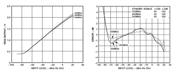
Figure 10: The data sheet of the AD8309 includes many tables and charts which define performance under various conditions, such as this pair which shows (left) RSSI output vs. input level, and (right) log linearity of RSSI output vs. input level; both for frequencies of 300 MHz, 400 MHz and 500 MHz and at +25°C. (Image source: Analog Devices, Inc.)
Another useful log amp is the Analog Devices AD8317, designed for wide bandwidth applications operating from 1 MHz up to 10 GHz. It can perform RF transmitter PA setpoint control and level monitoring, as well as power monitoring in radio link transmitters (Figure 11). While it can operate up to 10 GHz, it features 55 dB dynamic range up to 8 GHz with ±3 dB error, and enhanced temperature related performance with accuracy of ±1.0 dB and stability of ±0.5 dB over temperature.
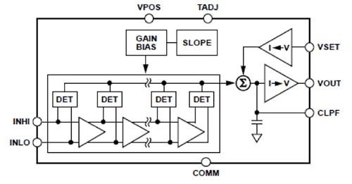
Figure 11: Analog Devices’ AD8317 is fully specified from 1 MHz to 8 GHz and has somewhat reduced but still useful performance to 10 GHz. It targets both transmit and receive path power monitoring situations. (Image source: Analog Devices, Inc.)
Among the many performance graphs in the data sheet is one that summarizes output error versus input level (Figure 12). There are many more with other perspectives and along multiple dimensions, including temperature, frequency, and power.
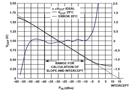
Figure 12: The basic performance of the AD8317 is initially characterized by this transfer function, which spans a 70 dB input power range; other graphs show performance at various frequencies and temperatures, among other factors. (Image source: Analog Devices, Inc.)
Of course, a part such as this needs other RF related specifications, as it targets operation beyond 1 GHz and reaching the 10 GHz region. For this reason, the data sheet provides the Smith chart for input impedance versus frequency (Figure 13). This information is essential for designing critical matching circuits and developing accurate simulation models at the highest frequencies.
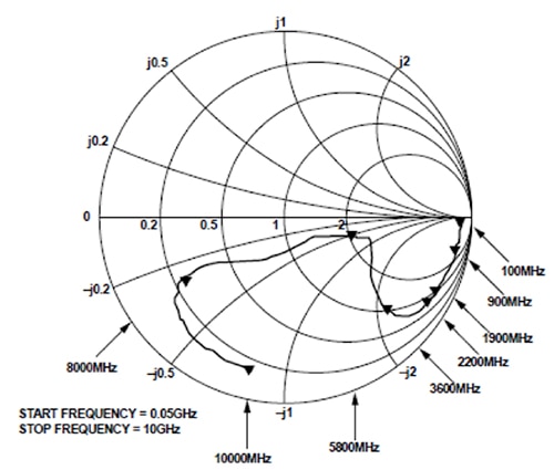
Figure 13: Comprehensive design, modeling, and simulation when using a GHz+ device, such as the AD8317, requires a Smith chart for computing input impedance matching requirements at all frequencies of interest. (Image source: Analog Devices, Inc.)
A final design caution: by their nature, log amps deal with signals having tiny amplitude, and their output is also very sensitive to any noise on the actual input signal. Therefore, careful PC board layout is mandatory, with:
- Generous bypassing of the DC power rails placed close to the log amp ICs.
- Minimization of opportunities for capacitive coupling of noisy signals or power lines into the input of the log amp.
- Use of the standard techniques for maintaining signal integrity on pc boards at high frequencies, including multilayer boards, ground planes, and ferrite beads.
Further, most log amps use differential input signals (and many also have differential outputs) to minimize common-mode noise, so any circuits that interface with the log amp must also be compatible with differential signals. Fortunately, most devices already use differential designs at these higher frequencies.
Conclusion
Despite the engineering focus on linearity in amplifier design (for good reason), there are applications where an amplifier with a nonlinear, accurate logarithmic input/output relationship solves challenging signal range problems. These log amps are used for received signal strength indication, power level control, and even to enable dynamic impedance matching for low VSWR between a PA output and its associated antenna.
Although log amps are more difficult to characterize and apply than conventional amplifiers, detailed data sheets show what they can do and how to realize the benefits they provide for their targeted applications.

免责声明:各个作者和/或论坛参与者在本网站发表的观点、看法和意见不代表 DigiKey 的观点、看法和意见,也不代表 DigiKey 官方政策。


