Two to Tango: MCUs Team Up with FPGAs
投稿人:电子产品
2014-01-08
Embedded designers spend a lot of time finding the right microcontroller (MCU) for a task at hand. Usually, space is a constraint and the right mix of raw performance, I/O, memory resources, power draw, and peripherals becomes the Holy Grail in the search for the right fit.
The search gets even more complicated if you have specialty logic that a specific design requires. Perhaps this is a “secret sauce” that your company knows how to make better than anyone else and makes the end products stand out. In this case the odds are that no one makes an MCU exactly the way you want it.
There is another option: a synergistic MCU and FPGA pairing. Highly-dense FPGAs can absorb so much logic that they can combine with micros, or even house micros, to do more than either part alone. In addition, the proprietary essence of your logic is hidden from prying eyes inside the FPGA.
This article discusses several options that allow designers to combine FPGA technology with embedded processors. We will examine monolithic approaches, systems-on-chip (SoC) solutions, stack-ups, and modules. All parts, datasheets, tutorials, and development tools referenced here can be found on DigiKey’s website.
Single-chip solutions
Micros can be made to run pretty fast. We are all familiar with multi-gigahertz processors at our fingertips. However, faster processors are typically more costly and harder to implement; PCB traces become transmission lines and tight impedance control is needed, especially on critical path signals. Not every design can shoulder the cost and time to develop with such devices.
This leaves lower cost, more general-purpose processors running at slower speeds as an alternative, more-economical choice for our designs. For non-demanding applications, this alone is good, but when the need for speed exceeds the micro’s cycle time, we have to make a choice. Software-based approaches cannot compete with the speed of a hard-logic implementation of a function. You can use discrete logic on a board, or couple the processor core with a pure logic resource like an FPGA.
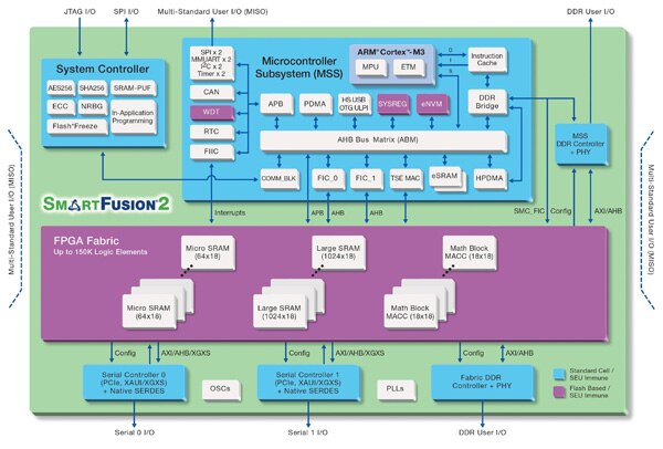
While real-time control and state-machine designs can be set up, controlled, and monitored fairly easily using simpler, less complex processors, there are times when higher-end peripherals, a wider data path, higher security, and faster executing speeds are needed. A good example of this level of processor horsepower is the Micro Semi SmartFusion2 family of parts like the M2S050T-FGG896, which is actually SoC based, combining hard IP blocks and FPGA on a single die. By leveraging hard IP within the device, engineers can maximize the functional resources common to many systems in minimal silicon space, while offering full flexibility for design customization with the FPGA fabric and firmware.
The 166 MHz ARM® Cortex™-M3 processor core is joined by many high-end peripherals like CAN, Ethernet, PCI Express, SERDES, and DDR functionality while coupling to an Actel Flash-based 50-Kgate Logic Module (Figure 1).

The ARM low-power core is coupled with Actel’s Flash Freeze real-time power-management system to achieve a 1 mW standby power rating compared to the still impressive 10 mW draw when all 50 K four-input look-up-table-based logic elements are powered up.
SmartFusion2 parts take aim at military, aviation, and space applications and are touted as high reliability and protected against single-event upset occurrences by using immune zero FIT Flash cells, protected memories, and ECC/EDAC protections. Encryption for 256- and 384-bit Advanced Encryption Standards (AES) and Secure Hash Algorithms (SHA) take advantage of a non-deterministic random bit generator to guard against predictable encryption codes.
Modular solutions
Modular solutions are also a valuable option and can use either lower-speed processors or high-end screamers. While the cost of modules is typically higher than single chip solutions, they provide faster time-to-market and prototype cycles, low-risk processor engines, and often mature and fully-functional development tools. They can also serve as a reference design when it comes time to roll your own for cost reduction purposes.
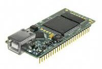
A good example of a modular solution that can easily be used for prototyping is the DIP-packaged DLP-FPGA module from DLP Designs (Figure 2). Here, a dedicated processor inside the USB link controller simply acts as the gateway into the Xilinx XC3S250E 250-Kgate Spartan® 3E FPGA. It uses a built-in configuration loader and can be a development tool itself. Power from USB or a target board can be used, and the module contains voltage regulators, RAM, and SPI Flash for auto configure at power up.

In addition, Mac-, PC-, and Linux-based systems can interface through a USB port to program the FPGA and configure the 40 I/O, on-board 128 Kx8 SRAM, and the SPI Flash. This part is ready for logic synthesis and uses a digital clock manager to assure clean, low-skew internal signaling. Training and tutorials are included to help you through the process of designing, loading, and running your design inside the FPGA.
Signal-processing modules
For signal processing, an adaptive or self-modifying design may need to combine high-speed Multiply and Accumulate functionality with a processor fast enough to model the analog world in the digital domain.
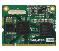
The L138-F1-236-RL MITYDSP from Critical Link (Figure 3) is a modular example with two processors, TI’s OMAP-L138 dual-core application processor offers a 456 MHz ARM926EJ-S MPU tightly coupled with a 456 MHz floating point TMS320C674x VLIW DSP, as well as a Xilinx Spartan-6 XC6SLX45 FPGA with up to 6,822 6-input Look Up Table logic elements supporting over 1 GHz data rates. It is designed to plug into a standard SO-DIMM-200 interface, and can operate in –40° to +70°C extended temperature environments.

This is a very capable little module. On board are 10/100 EMAC MII/MDIO Ethernet interfaces, two USB ports, SATA and MMC/SD memory card interfaces, video-in and video outputs, along with 96 I/O lines. JTAG development channels let you quickly load, test, emulate, and debug your designs. The processor environment supports QNX, Linux, Windows, and ThreadX real-time operating systems (RTOS) and it has lots of Flash (512 Mbytes of NAND and 8 Mbytes of SPI NOR) and RAM (256 Mbytes of DDR2).
The modular nature of these processor and logic engines means multiple units can be plugged into a single motherboard for expandable, scalable, and parallel-processing applications.
Another module designed to be used in a parallel-processing environment is available for test and development via the Cognimem 901-1001 SDK development board using the Cogniblok-4K Neuron processor. These are configurable and stackable pattern recognition modules that are designed to be paralleled for complex tasks like pattern recognition and running process-intensive algorithms.
The combination of an AI processor and FPGA with 4 Mbytes of High-Rel Magneto RAM (MRAM, based on giant magneto resistance, which is immune to EMI, RFI, and EMP conditions) from Everspin Technologies lets these blocks interconnect in parallel, multiaxis configurations to do cognitive computing, sensor fusion, video analytics, and more. Once the pipeline is filled, complex tasks can be achieved in virtual real-time. An independent USB coprocessor bridges the board to USB for rapid development and downloading.
In summary, the combination of a micro with an FPGA can allow a high degree of flexibility and performance, as well as simplify updating. This is especially useful for adaptive algorithms, developing new technologies, and in any designs where you expect to be refining an algorithm or process technology as you get higher up on the learning curve.
For more information on the parts discussed in this article, use the links provided to access product information pages on the DigiKey website.
免责声明:各个作者和/或论坛参与者在本网站发表的观点、看法和意见不代表 DigiKey 的观点、看法和意见,也不代表 DigiKey 官方政策。


 中国
中国