Capacitor Selection is Key to Good Voltage Regulator Design
投稿人:电子产品
2014-06-24
Modular DC-DC switching voltage converters (or voltage regulators) are fully integrated devices that take away most of the complexity of power supply design — but not all. One of the key areas that are still left to the design engineer’s discretion is the choice of components for, and layout of, the energy storage and filtering circuits. In principle, these look like simple circuits comprising a few resistors, capacitors, and the energy-storage element, usually an inductor.
However, this simplicity belies the fact that the vast majority of problems associated with switching regulators have nothing to do with the module itself, rather the improper use of capacitors in the input filter and energy storage and filtering circuitry. Choosing the wrong type of capacitor, getting the required capacitance just slightly incorrect or misplacing the passive device can cause an otherwise perfectly functioning voltage regulator module to generate excessive electromagnetic interference (EMI). In a worse-case scenario, poor capacitor selection can result in a good voltage regulator becoming unstable and failing prematurely.
This article describes how to select the correct capacitors for the external circuitry of modular voltage regulators and describes what can go wrong if a poor choice is made.
Dealing with EMI
Switching voltage regulators have become popular because they are efficient and flexible. However, there is a trade-off. The chips are more expensive, take up more space, have a relatively slow transient response to load variances, and, because of the switching operation, it can be difficult to prevent EMI from the switching circuit radiating out into both input and output sides of the device.
The best way to tackle EMI is to target the source, which in a switching regulator is typically the power Field Effect Transistor (FET), particularly when it turns off. Figure 1 shows a basic step-down (“buck”) regulator. When the power FET (“Q1”) is on, current flows around the circuit as indicated by the arrows. When Q1 is turned OFF, the voltage on the end of the inductor closest to Q1 is forced to swing negative until the diode responds by turning on to hold the current through the inductor constant. However, because the diode cannot switch-on in zero time, the voltage can overshoot beyond the diode drop and then ripple (or “ring”) as the diode eventually turns on. Even if a Schottky diode is used, parasitic trace inductance will still cause some rippling to occur. This rippling generates EMI in the 20-100 MHz range.
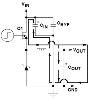
Figure 1: Basic buck-switching voltage regulator circuit showing current flow when Q1 is on (Courtesy of Texas Instruments).
A proven way to reduce EMI caused by ringing is to add an R-C “snubber”, comprising a ceramic capacitor plus carbon film resistor, close to the FET as shown in Figure 2. The snubber works because when the FET switches off and stops sourcing current, the snubber capacitor sources enough current such that the rate of current change through the inductor is slowed, lowering the incidence of rippling in the diode. Providing the component values of the snubber circuit are appropriately selected, they will damp any rippling that does occur.
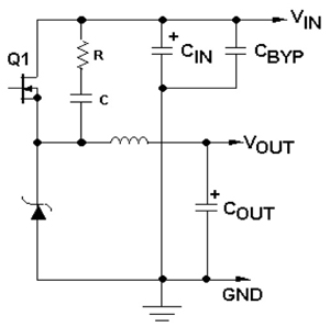
Figure 2: R-C snubber circuit helps to reduce EMI radiating from power FET (“Q1”) (Courtesy of Texas Instruments).
The R-C snubber circuit can reduce overall voltage regulator efficiency by a few percentage points. The loss of efficiency shows up most at light loads because the power expended in the snubber is relatively constant and independent of output-load current.¹ (Some newer switching voltage regulator modules integrate the R-C snubber into the chip, saving the design engineer the task of coming up with a suitable circuit.)
In addition to the EMI-reducing R-C snubber circuit, the design engineer also needs to select a capacitor at the front end of the device to minimize the input-voltage variations caused by the discontinuous input current of a switching-voltage regulator.
The value of the input capacitance is not the main consideration when selecting this capacitor; rather it is the RMS current and the voltage rating.
The RMS current of the input capacitor (CIN) can be calculated from:
where D is the PWM square-wave duty cycle.
The worst case occurs at D = 50 percent (i.e., VIN = 2 x VOUT), which yields IIN,RMS = IOUT/2.
The equivalent series resistance (ESR) of the bulk-input capacitor causes the device to heat up under this RMS current. Higher ESR increases heating, so a good place to start is to specify a device with as low an ESR as possible within the constraints of the budget.
Ceramic and tantalum capacitors are both suitable as input capacitors for switching voltage regulator circuits. Choose ceramic capacitors with a voltage rating of at least 1.5 times the maximum-input voltage. If tantalum capacitors are selected, they should be chosen with a voltage rating of at least twice the maximum-input voltage.
A small ceramic capacitor in parallel to the bulk capacitor is recommended for high-frequency decoupling.
The L-C output filter
Perhaps the most important capacitor choice a power supply design engineer can make is the selection of the component for the voltage regulator’s L-C output filter. The job of this circuit is to filter the voltage square wave at its input (the switching node) to produce a constant regulated voltage at its output (VOUT).
In a buck converter under steady-state conditions, the average current in the inductor (IL) is equal to the output current IOUT. Due to the input being a square wave, the inductor current is not constant, but ripples between a maximum and a minimum value as the input voltage switches on and off. The difference between the maximum and minimum (ΔIL) is called the peak-to-peak inductor current ripple (Figure 3).
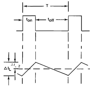
Figure 3: Inductor current ripples in response to voltage-input square wave.
In the L-C output filter, the role of the capacitor is to maintain a constant output voltage (VOUT) and limit any voltage spikes. In practice, it is virtually impossible to eliminate voltage variation around the target value and this manifests itself as an oscillation between a maximum and a minimum value, whose difference (ΔVOUT) is called the peak-to-peak voltage ripple. Voltage ripple is a function of the inductor ripple current, the switching frequency, and the output capacitor’s ESR.
The design engineer should specify the maximum current- and voltage-ripple for the circuit depending on the application. The inductor is typically selected to keep the ripple current to less than 20 to 30 percent of the rated DC current. Sensitive modern silicon circuits require tighter control of voltage ripple typically in a 5-100 mV range. Figure 4 illustrates acceptable voltage ripple profiles for a buck regulator delivering a 2.0 V output.
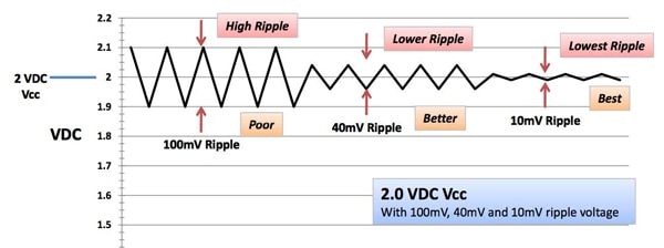
Figure 4: Lowering voltage ripple improves downstream circuit performance (Courtesy of Texas Instruments).
Selecting the best capacitor for a switching voltage regulator’s output filter is not a trivial task. However, a good starting point is to estimate the maximum ESR and minimum capacitance for a given output voltage ripple. The ESR can be calculated from the formula:
And the minimum output capacitance (COUT) can be estimated from the following equation:
Where ΔVOUT, overshoot is the maximum voltage overshoot allowed on the output and IL, max is the maximum inductor current.²
However, there is a little more to the output capacitor selection than that. Even a device with an apparently correct ESR can suffer overheating if the input “ripple current rating” is not taken into consideration. Prolonged exposure to high temperatures can cause a gradual evaporation of the device’s liquid electrolyte through the seal, raising ESR, and causing even more heating in a vicious cycle that leads to capacitance drop and ultimately failure. The core temperature rise should be limited to 5-10°C to prevent such damage.
The power dissipation (PCAP) of the output filter circuit capacitor is:
Where IRMS is the input ripple current.
In other words, for a given ESR, the internal temperature rise is proportional to the square of the ripple current.
It is important to note that ripple current rating can vary widely between technologies, manufacturer, and voltage for a given capacitance. High-ripple current-rating capacitors tend to have low ESR, greater surface area, and a high-heat transfer constant. Tall capacitors of equal volume to short, fat devices dissipate heat better because the heat is transferred from the core to the case more easily. Nonetheless, capacitor size compared to ESR rating also varies widely for different capacitor technologies and even between the same technologies from different manufacturers. The design engineer is advised to carefully familiarize oneself with the spec sheet for a shortlisted device before making a selection.
Another important factor is placement of the output capacitor on the PCB. It is a good idea to keep traces short for high-frequency switching circuits to minimize EMI. It is also a good idea to make sure that the capacitor is not sited too close to sources of heat, such as diodes, as this is likely to raise the internal temperature of the device even higher.³
Seeking guidance
Help is at hand for design engineers looking to source the correct external capacitors to work with the many switching voltage regulator modules on the market.
The spec sheets that accompany and describe the module maker’s products typically include applications circuits that suggest capacitor values for the input- and output-filter circuits for the devices.
Consider Texas Instruments’ (TI) TPS53318. The chip is a synchronous buck-switching voltage regulator that features an adjustable switching frequency from 250 kHz-1 MHz. The device features a wide conversion input voltage range (4.5-25 V), very-low external component count, auto-skip-mode operation, internal soft-start control, and no need for compensation. The TPS51462 offers an output voltage range of 0.6-5.5 V (at up to 8 A output current) and is available in a 5 x 6 mm, 22-pin, QFN package.
The data sheet for TI’s TPS53318 provides an application circuit diagram and the company helpfully suggests typical capacitance values for the output filter circuit. Further on the data sheet includes a very detailed design procedure that describes how to select the inductor, set the output voltage, determine the output capacitance, and check the power supply’s output stability for a given output capacitor.
Linear Technology’s data sheet for its LTC3549 switching buck voltage regulator includes an application circuit advising on values of input and output capacitors (Figure 5).
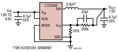
Figure 5: An application circuit for Linear Technology’s LTC3549 advises values for input and output capacitors.
The data sheet also includes some handy design tips on external component selection such as pointing out that ripple-current ratings are often based on just 2,000 hours of life, so it can make sense to specify a capacitor with a higher temperature capability than required. In addition, Linear Technology’s spec sheet advises that because the LTC3549’s control loop does not depend on the capacitor’s ESR for stable operation, ceramic devices can be used (with care) to achieve very-low-output ripple and small circuit size.
The LTC3549 employs a fixed operational frequency of 2.25 MHz. The 1.6-5.5 V input voltage range makes the device ideally suited for single-cell Li-Ion, Li-Metal, Alkaline, NiCd or NiMH battery-powered applications. Burst Mode operation can be user-enabled, increasing efficiency at light loads, further extending battery life.
For its part, STMicroelectronics explains that the input capacitor must have an RMS current rating higher than the maximum RMS input current and an ESR value compliant with the expected efficiency in its data sheet for the ST1S31 synchronous-buck switching regulator. Further, the data sheet advises that on the output side for a ceramic (MLCC) capacitor, the capacitive component of the voltage ripple dominates the resistive one, while for an electrolytic capacitor the opposite is true. The company’s data sheet includes all the relevant formulas for calculating capacitor values and provides advice on which manufacturers supply suitable components.
The ST1S31 is an internally compensated, 1.5 MHz synchronous-buck voltage regulator that operates from a 2.8-5.5 V input, regulating an output voltage from VIN to as low as 0.8 V. The chip features a peak current mode control with internal compensation and is claimed to deliver a very compact solution with a minimum component count. The device is available in 3 x 3 mm, 8-lead VFDFPN and SO8 packages.
A critical part of power supply design
Considering the sophistication of contemporary switching voltage converter modules, the choice of input and output capacitors for the chip’s filter- and energy-storage circuits would seem to be a trivial part of power supply design. However, nothing could be further from the truth.
An incorrect choice of technology, dimensions, capacitance or ESR can see the lowly capacitor at best ruin the circuit’s efficiency and at worst lead to premature product failure. The recommended approach is to use the wealth of information supplied in the vendors’ datasheets to calculate initial capacitance and ESR values and then test the prototype circuit with several alternative devices across a range of technologies.
For more information on the parts discussed in this article, use the links provided to access product information pages on the DigiKey website.
References
- “Engineers note: Capacitors are key to voltage regulator design,” Texas Instruments, SNOA842, 2011.
- “Selecting L and C Components in the Power Stage of the MC34700 Switching Regulators,” Giuseppe Maimone, Freescale Semiconductor Application Note AN4067, November 2010.
- “Efficiency and Power Characteristics of Switching Regulator Circuits,” Brian Huffman, Linear Technology, Application Note 46, November 1991.
免责声明:各个作者和/或论坛参与者在本网站发表的观点、看法和意见不代表 DigiKey 的观点、看法和意见,也不代表 DigiKey 官方政策。


