Reduce Design Complexity Using Integrated Isolated Flyback Converters
投稿人:DigiKey 北美编辑
2016-11-02
Galvanic isolation is a critical requirement for power supplies in applications designed to work with high voltages or in close proximity to humans. Flyback converters offer an effective isolated power solution, but can present significant design challenges to ensure stable output across a wide load range.
To help overcome these challenges, we will describe the issues and then use a specific model converter as an example to specify some of the factors to consider in order to realize a successful design.
The challenges associated with producing an efficient power supply based on flyback topology require the knowledge of experts in power design. Today's demand for faster delivery of smaller, simpler designs exacerbates the difficulty of working with traditional approaches. For designers, newer integrated devices such as the ROHM BD7F series offer an effective solution for less complex designs with a faster time to market.
Among converter topologies, the flyback converter offers isolation, and requires relatively few parts even in discrete designs. Fundamentally, a flyback converter is a buck-boost converter utilizing a transformer. While the flyback converter's switching topology enables output regulation, its transformer provides galvanic isolation and enables you to select the input/output voltage ratio by selecting an appropriate winding ratio.
Flyback feedback
In operation, current flow across the primary side of the flyback converter's transformer causes energy to be stored in the transformer. When the converter's power switch turns off, the stored energy is transferred to the output. To regulate its output, a flyback converter uses a feedback circuit that compares the output voltage level with the desired voltage value and adjusts the output accordingly. To isolate the feedback loop itself, conventional isolated flyback-type supplies use optocouplers (Figure 1 Top) or auxiliary windings of the transformer (Figure 1 Bottom).

Figure 1: Conventional flyback converters regulate their output using feedback loops isolated with optocouplers (Top) or auxiliary windings (Bottom). (Image source: Texas Instruments)
The emergence of highly integrated flyback controllers offers a significant advantage to anyone who needs to create smaller isolated supplies. While these controllers reduce parts count compared to many alternative solutions, they do require an external FET as the power switch. The controller drives the external FET to control the output voltage of the power supply.
In contrast, converters such as the Texas Instruments LM5001 (Figure 1) integrate the FET switch for even further parts-count reduction and smaller total solution size. This higher integration comes at a price because the internal FET switch constrains the maximum voltage and peak current that the converter can handle. For example, the LM5001 converter is specified with voltage and current limits of 75 V and 1 A, respectively.
However, for many mobile and IoT designs, more recent converters such as the ROHM Semiconductor BD7F200 (10 W output at 24 VIN) and BD7F100 (5 W output at 24 VIN) offer an even more compelling advantage with their ability to further simplify designs and reduce parts count even more dramatically.
This reduction is possible because these devices are able to detect the secondary side voltage and current from the primary side, eliminating the need for separate optocouplers, or transformers with tertiary windings. Consequently, you can create an efficient isolated power supply using only a simple transformer and a few additional passive components (Figure 2).

Figure 2: ROHM BD7F isolated converters use primary-side sensing to regulate voltage output. (Image source: ROHM Semiconductor)
Isolated flyback converter designs based on these parts offer greater size reduction, reliability, and energy savings. To speed development, ROHM offers a fully configured evaluation board to help customers apply these integrated solutions into their own designs (Figure 3).

Figure 3: The ROHM Semiconductor BD7F100HFN-EVK-001 evaluation kit. (Image source: ROHM Semiconductor)
Monolithic converter
Traditional flyback converter designs typically use an error amplifier to correct their output voltage. In contrast, the BD7F series uses an approach called adaptive ON-Time control that is based on a comparator. During operation, the circuit determines ON and OFF times by comparing its internal reference voltage with the feedback voltage monitored at its SW terminal (Figure 4).

Figure 4: The ROHM BD7F series adaptive ON-Time controller relies on a comparator that senses primary side feedback voltage to adjust switch duty-cycle as needed to maintain a stable output voltage. (Image source: ROHM Semiconductor)
The adaptive ON-Time control method offers significant advantages in output stability. In fact, the devices are able to limit output voltage fluctuations to 200 mV at a load current of 1 A and rise time of 100 μs. As a result, these devices respond quickly to load transients, reducing output fluctuations (Figure 5).

Figure 5: The adaptive ON-Time control method used in the ROHM BD7F isolated converters helps ensure that output voltage fluctuations (lower waveform) are limited to about 200 mV during load transients (upper waveform). (Image source: ROHM Semiconductor)
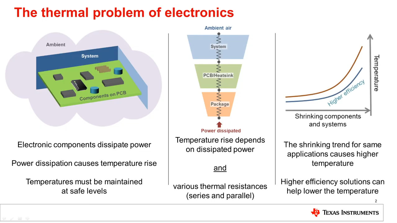
Using this control method, the converter ultimately delivers VOUT according to the following:
Eq.1:
where
RFB is the external resistance between the FB-SW terminals
RREF is the external resistance between the REF–AGND terminals
NP is the number of turns in the transformer primary side
NS is the number of turns in the transformer secondary side
VREF is the REF terminal voltage
VF is the forward voltage VF of the output diode
IS is secondary transformer current
ESR is the total impedance in the secondary side
A notable result illustrated in this equation is that you can in part set the output voltage by choosing the appropriate primary and secondary turns ratio of the transformer, and by adjusting the ratio of the resistances RFB and RREF.
The equation further illustrates that the output voltage level is also subject to an output voltage error determined by VF and ESR. This error can be reduced by selecting a Schottky barrier diode with a small VF. The ESR, however, is more difficult to control as it is the total impedance in the secondary side, which includes the transformer wirewound resistance and the pc board impedance.
Even with optimal diode selection and careful ESR management, it is possible to have an output voltage error in your application, which in turn can lead to poor load regulation. To reduce the effect of these inherent error sources, BD7F devices are designed with an internal load compensation function that can significantly improve output regulation across the device's output current range.
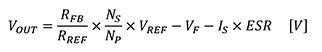
The load compensation factor is set using a resistor and capacitor connected to the device's COMP pin. The capacitor CCOMP helps stabilize VCOMP (see Figure 4). ROHM recommends using CCOMP values from 0.01 μF to 0.1 μF. In choosing RCOMP, the required resistance value can be estimated using the following equation:
Eq.2:
where:
RVFis diode forward resistance, approximating the change in Vf due to Is
ESR is the total impedance in the secondary side
K is the compression magnification term (defined as 1/50k in this case)
RFB is the external resistance between the FB-SW terminals
NP is the number of turns in the transformer primary side
NS is the number of turns in the transformer secondary side
Although this equation provides a theoretical value for RCOMP, the various resistances (RVF, RFB, and ESR) are dependent upon the details of the design, components, and pc board. Consequently, you need to determine the actual value of RCOMP by measuring VOUT across the application's load-current range and adjusting RCOMP accordingly.
Practical considerations
Along with its many advantages, the flyback topology does suffer a disadvantage. Large transient voltage spikes can often occur at the drain of the power switch and at the secondary rectifier. These voltage spikes arise from the transformer's inherent leakage inductance associated with the small amount of energy stored in the imperfectly coupled windings.
In the BD7F devices, ringing can occur at the SW pin when a spike occurs or when the integrated MOSFET turns OFF. Furthermore, when the MOSFET turns ON, a reverse spike voltage can occur in the output diode. Consequently, you typically need to add a simple snubber circuit to control the effects of the leakage inductance and improve the reliability of the power supply.
Conclusion
The flyback converter topology offers isolation and requires relatively few additional components to produce a fairly efficient power supply. However, traditional methods for regulating these converters have required the use of optocouplers or complex transformers with tertiary windings.
In contrast, newer integrated converters such as the ROHM BD7F series achieve output voltage regulation without the need for these additional components. Using these devices, efficient isolated power supplies can be created with fewer additional components, offering greater reliability in a smaller footprint.
免责声明:各个作者和/或论坛参与者在本网站发表的观点、看法和意见不代表 DigiKey 的观点、看法和意见,也不代表 DigiKey 官方政策。