Multicore MCUs for Real-Time Control
投稿人:电子产品
2013-10-16
Single-core microcontrollers can multitask if the timing is well defined and the time-critical functions are partitioned so that interrupts and timer-service routine response times are fast enough to handle the tasks at hand. However, it is the design equivalent of juggling. While one ball is in the air not needing service, another may need service right away to keep the process moving. As long as you are fast enough to switch contexts, all is well.
When tasks overlap, it may be impossible to react quickly enough, such as when several synchronous and asynchronous stimuli hit at once. In these cases, there are only a few options. One is a faster processor. Another is to use multiple processors and partition the application into time manageable or pipelined chunks. A third, and in many ways the best, choice is to employ a single-chip dual-core or multicore processor.
This article looks at processors with more than one core. These parts permit task executives to assign individual responsibilities to each core so that other distractions do not take away from the real-time performance necessary to accomplish tasks such as time-critical control loops. All parts, datasheets, tutorials, and development kits referenced here are available on DigiKey’s website.
Back of the bus
The key to understanding how to best choose a dual-core or multicore processor is how it uses or replicates resources. The most straightforward (and a very effective) approach is for each processing core to have its own “support staff,” including its own program and data memory, clock, and I/O. Shared peripherals would need to be claimed by the processor core currently using them (Figure 1), and dual-port memory serves well as an means of exchanging critical data.
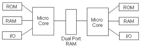
Shared resources can save die area and power, but must be synchronized in such a way that they are always available to each processor core. A floating-point processor may require several instructions and cycles to load operands, then process and store. In both cases discussed so far, holding a different core in a wait state until the resource is free is not an effective approach and more or less drops performance down to single-core level during these conditions.
The same is true with common data path resources like a data bus. If there is only one data bus internally, each core will need access to it, usually at least one time each cycle, but sometimes more. A wait state can be inserted when there is contention, but this does not help the cause.
As you may have surmised, the synchronicity and timing of the internal cores is an important factor. If each core is running at its own frequency with its own clock, access to a shared bus can be hit or miss.
However, if the micro state is staggered between cores using a common clock, maximum utilization of internal resources can take place without any contention. Taking a Von Neumann architecture as an example, we can have four core processors share a common bus using fetch, decode, operate, and execute cycles (Figure 2). Note that while stage 2 and 3 operations can be internal to each processor, an execute cycle that uses the bus (like a memory store) can still cause contention. Some I/O operations during an execute cycle can be done if the I/O path is unique to the processor.

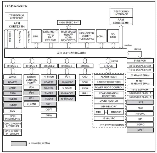
Another factor to keep in mind is that every core processor in a part does not have to be identical or equal. NXP Semiconductors' 32-bit asymmetrical dual-core 204 MHz PC4337JBD144E is a member in the company’s LPC43xx family of ARM® Cortex™ M4 and M0 cores in a single package. The parts vary in ROM, RAM, peripheral mix, I/O, and packages size, but all feature a smaller M0 core to take over housekeeping, initialization, and data management chores while the M4 core is free to do more process-intensive functions, thanks to its floating-point hardware and DSP extensions.
The NXP parts use a multilayer matrix and individual peripheral bridges to solve arbitration issue between processor cores and peripherals (Figure 3). A Master and Slave designation also ensure prioritization. The idea is that the AHB matrix connects the ARM Cortex M4 buses and other bus masters to peripherals in such a way as to allow peripherals that are on a different slave port to be accessed simultaneously by different bus masters.
Freescale’s i.MX 6 is a family of scalable single-, dual-, and quad-core 32-bit ARM 9 processors. Their cores each run at 1 GHz clock speeds, and like other high-end processors, the parts feature hardware support for peripherals like USB (and OTG), Ethernet, MMC/SD card, PCI, 2D and 3D graphics, and SATA to name just a few (Figure 4).
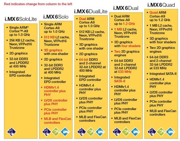
Take Freescale’s dual-core MCIMX6D5EYM10AC in a 624-pin FBGA package. Its 0.9 to 1.5 V operations keep heat and power dissipation to a minimum, not an easy task with 224 I/O. While a chunk of this I/O is dedicated to the external program memory via an external bus interface, these parts nevertheless are very dense with a very-high transistor count, so keeping power low is critical.
It should be noted that these cores are not asymmetrical. They are virtually identical. This means that a single-core design can migrate to a dual- or quad-core design and code will be compatible as the performance scales up. This can be a key decision factor, especially if you are designing a notebook, smartphone, laptop, or other multifunction device that needs to support many high-end peripherals simultaneously.
Another player in the multicore MCU arena is XMOS, which provides a family of scalable 32-bit parts. The XS1 family includes single, dual, quad, hex, and octal cores, as well as up to 16-core parts ranging from 48-pin TQFP packages to 512-pin LFBGA packages (Figure 5). These parts also contain a rich set of peripherals and features. Consider the 0.95 to 3.6 V 48-pin 400 MIPS quad-core XS1-L4A-64-TQ48-C4. Each core (known as a tile), executes real-time tasks simultaneously and can execute computational, advanced DSP code, control code, or software that handles I/O.
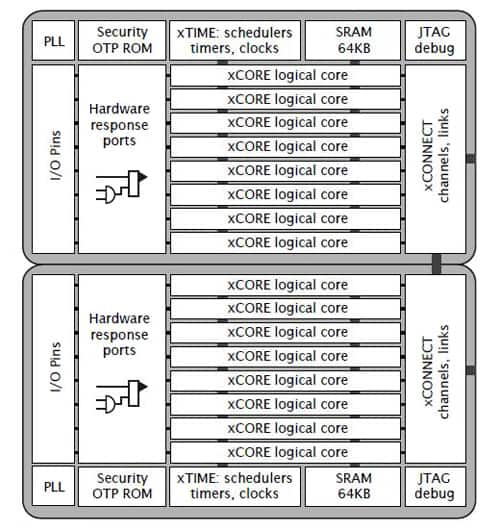
In the XMOS, parts-scheduling hardware performs RTOS-like functions to ensure low latency and eliminate interrupts, ensuring deterministic operations. Since each core is identical, as computational and multitasking needs grow, so can the capabilities of your design, without having to start over creating software.
In summary, clever partitioning of processors and functions can streamline a design, and multicore parts can be a key element to help engineers tackle critical real-time demands. Many well-engineered parts and tools are readily available to help. For more information on the parts discussed in this article, use the links provided to access product pages on the DigiKey website.
免责声明:各个作者和/或论坛参与者在本网站发表的观点、看法和意见不代表 DigiKey 的观点、看法和意见,也不代表 DigiKey 官方政策。
