Adding Energy Measurement Features to IoT Designs
投稿人:电子产品
2016-04-19
Adding power measurement to a microcontroller-based Internet of Things (IoT) design can be simple if the MCU features an integrated analog-to-digital converter (ADC). Ensuring accurate results, however, can be a challenge. Engineers can meet these challenges with a few additional components and some extra processing — or even turn to dedicated energy-measurement devices to handle more complex requirements.
Energy measurement has emerged as an increasingly important feature of connected products including grid-friendly equipment, smart plugs, and home appliances, among a growing list. Besides offering a competitive differentiator, energy measurement is a key factor in sophisticated automation systems able to detect abnormal power usage patterns related to maintenance problems. Indeed, smart home appliances offer consumers more than the convenience of receiving an alert when clothes are ready to be removed from the dryer. By providing information on energy usage patterns throughout the household, these products not only help consumers optimize their energy usage but also warn of potential breakdowns, allowing users to employ preventative maintenance measures to avoid later higher costs — and greater inconvenience.
Leveraging integrated MCUs
Conceptually, building an energy-measurement feature in an MCU-based design is simple enough: By repeatedly sampling instantaneous voltage Vi and current li, instantaneous power is simply calculated as the sum of the product VIN x IIN x 𝑐𝑜𝑠 (𝜑), where φ is the phase difference between the voltage and the current (Figure 1). (For the purposes of basic measurement of energy consumption, some applications can even ignore phase differences, further simplifying requirements.)
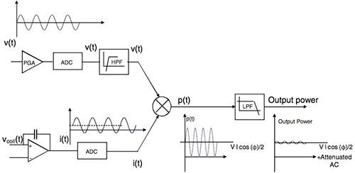
Figure 1: In principle, an MCU-based IoT design can manage the incremental processing load associated with basic power calculations. (Courtesy of STMicroelectronics)
MCUs with an integrated ADC offer a cost-effective solution for implementing a low-parts-count energy-measurement feature in a smart appliance — or any IoT design using one of these devices. In theory, the designer need only sample line voltage and current to calculate power, store the results for local display, or transfer them upstream to the cloud or to a local controller such as a home automation management node. In practice, however, the very simplicity of this approach gives rise to additional design challenges.
A typical MCU-integrated ADC will not provide the dynamic range or resolution required for the line voltage and current measurement, but accurate measurement of these values is critical. Indeed, significant errors in these initial values will compromise the results of simple power calculations much less than more involved calculations of other energy characteristics. Consequently, designers will need to add amplifiers and other conditioning elements to provide a useful signal matched to the ADCs dynamic range (Figure 2). In addition, power measurements typically measure current on both the active line and the neutral line to help detect any fault conditions. Finally, bandpass filters, transient voltage suppression diodes, and isolators, among other components, might be required depending on the application.
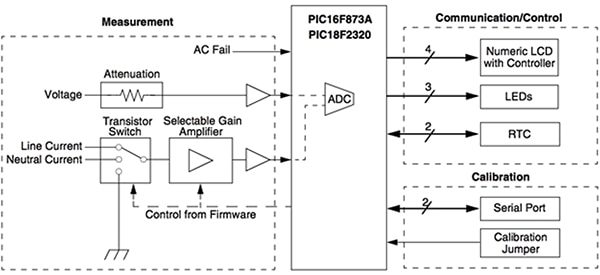
Figure 2: To implement power measurement using the ADC integrated in a typical MCU used for IoT designs, engineers often only need to add a few components for signal conditioning and control. (Courtesy of Microchip Technology)
As shown in Figure 2, an MCU such as the Microchip PIC16F873A or PIC18F2320 controls gain of an input amplifier and alternates selection of the active line and neutral line for current measurement.
ADC limitations
Even with the additional components, the use of an MCUs integrated ADC is an effective approach for non-utility energy measurement. Yet, power calculations require voltage and current to be sampled at precisely the same time — a requirement that conflicts with availability of the single ADC that is embedded in a typical low-cost MCU. With a single ADC, the time that voltage and current measurements are taken will differ by some time tm as ADC input is switched from the voltage-sense line to the current-sense line. Although time tm might be significantly reduced with a multiplexed high-speed ADC combination integrated on more expensive MCUs, the same conflict applies even with these devices.
Designers can use interpolation techniques to address this difference — measuring voltage immediately before and after a single current measurement (or conversely, taking current measurements before and after a single voltage measurement). If the time between the two bracketing measurements (corresponding to ~2tm) is reasonably short, the segment of the voltage curve bounded by the two bracketing voltage samples will be linear within the system’s margin of error. Consequently, linear interpolation provides a reasonable approach for estimating the voltage value at the exact time the current measurement was taken.
Enhanced measurement
Many IoT designs are likely to be based on a low-cost MCU with an integrated ADC. Furthermore, many IoT applications impose a relatively low duty cycle on MCU operation — leaving MCU cycles available for basic energy calculations. Consequently, designers can often add a reasonably accurate energy-measurement feature with minimal impact on the cost and size of the IoT device itself.
If energy measurement is a primary requirement, selection of an MCU with enhanced sampling capabilities is another option. For example, the Texas Instruments MSP430I2xx MCU series includes devices that integrate multiple independent differential input 24-bit sigma-delta ADCs (for example, two ADCs on the MSP430I2020 and four ADCs on the MSP430I2041). The ADC's operate in a synchronous manner, but the hardware actually allows the sampling times to be offset in finely controllable steps to correct any phase shift between the voltage and current signals.
If other design requirements prevent use of this type of MCU, designers can instead turn to dedicated ADCs, but parts count begins to rise to accommodate the required amplifiers and other components needed to condition the signals for optimal conversion by the ADCs. A multichannel analog front-end (AFE) device such as the Microchip Technology MCP3901 can offer a more effective solution and, in many cases, simplify design by integrating the full signal path required for signal conditioning and conversion.
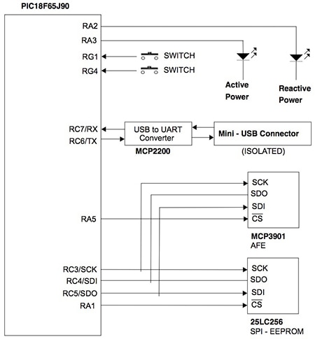
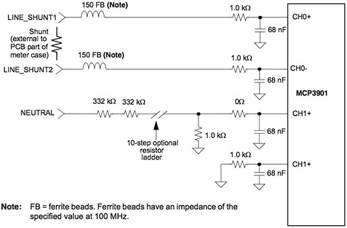
The MCP3901 is a dual-channel AFE containing two synchronous sampling delta-sigma ADC, two programmable gain amplifiers, a phase-delay compensation block internal voltage reference, modulator output block, and high-speed 20 MHz SPI compatible serial interface. The device’s high level of integration lets designers implement energy measurement with only a few components in simple system designs (Figure 3). In the figure, the MCP3901 uses a simple analog input circuit and minimal digital interface to work with a Microchip PIC18F65J90 MCU, 25LC256 EEPROM, and MCP2200 digital interface.
|
|
|
| (A) | (B) |
Figure 3: The Microchip MCP3901 AFE helps simplify energy-measurement design, providing a simple digital interface (A) while requiring only a few additional components for the analog input (B). (Courtesy of Microchip Technology)
In adding energy-measurement functionality to an MCU-based IoT design, an AFE can help reduce parts count. On the other hand, it still adds a processing load to the primary MCU. As noted earlier, IoT devices with low-duty-cycle requirements might easily handle the additional processing required for energy measurement. If the additional functionality includes calculations of more sophisticated energy characteristics, however, the MCU might face a prohibitive processing load. In these cases, designers can deliver sophisticated features, enhance accuracy, and nevertheless still simplify design by using dedicated energy metrology ICs such as the Maxim Integrated 78M6610+LMU. These devices integrate multiple complete signal chains and a processing core dedicated to executing energy calculations from on-chip storage (Figure 4).
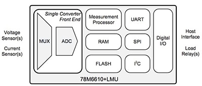
Figure 4: Devices such as the Maxim 78M6610+LMU provide a single-chip solution for energy measurement, integrating the signal chain with a processor dedicated to calculating power characteristics. (Courtesy of Maxim Integrated)
The Maxim 78M6610+LMU provides a flexible sensor configuration of four analog inputs and includes phase compensation registers that allows developers to compensate for phase errors or time delays between the voltage input source and respective current source that are introduced by the off-chip sensor circuit. The internal 24-bit processor uses the chip’s field-upgradeable firmware to perform all the necessary signal processing, compensation, and data formatting for accurate real-time measurement.
The 78M6610+LMU not only calculates instantaneous active power but also generates more complex power characteristics, including instantaneous reactive power, average active power, average reactive power, apparent power, and power factor. Furthermore, the device includes the ability to separate low-rate voltage, current, active power, and reactive power measurement results into fundamental and total harmonic components. These outputs can also be used to track individual harmonics as well as the total value excluding the selected harmonic. The Maxim Integrated 78M6610+LMUEVK evaluation kit includes a comprehensive set of design resources including full schematics to help jumpstart design with this device.
Conclusion
As energy measurement plays a growing role in connected smart products, designers must contend with new requirements to upgrade existing designs with basic power measurement features or implement more sophisticated capabilities in new designs. In many cases, developers can include power-measurement capabilities by leveraging the ADC integrated in many MCUs already in use in IoT designs. When the IoT design’s MCU cannot be used in this role, designers can turn to highly integrated AFEs or even dedicated energy metrology ICs able to deliver complex energy-measurement characteristics with minimal impact on IoT design cost, package size, or delivery schedule.
For more information about the parts discussed in this article, use the links provided to access product pages on the DigiKey website.
免责声明:各个作者和/或论坛参与者在本网站发表的观点、看法和意见不代表 DigiKey 的观点、看法和意见,也不代表 DigiKey 官方政策。
